

1 Introduction
As society seeks to address the growing demand for energy while also tackling pressing environmental challenges, the advancement of innovative and novel technologies plays a vital role in ensuring our future sustainability and progress.[1-5] Current focuses include water splitting for hydrogen production, [6-11] the implementation of fuel cells for electricity generation, and the advancement of battery technologies for efficient energy storage.[12-21] The efficient utilization of electrical energy through advanced conversion and storage technologies presents significant opportunities for fostering a sustainable future.[22-26] The transition from fossil fuels to clean, sustainable energy solutions faces significant challenges, with large-scale electrical energy storage being a primary concern. One effective method for storing energy involves the electrochemical conversion of inert molecules, such as H2O, CO2, and N2, into higher-value chemicals.[27-30] Therefore, efficient catalysts play a crucial role in advancing both energy conversion and storage technologies.[31-37] The performance optimization and mechanism studies are essential in these important areas.[38-46] Conventional electrochemical methods present several limitations in effectively investigating catalytic mechanisms and optimizing performance.[47-50] Firstly, these methodologies often emphasize the statistical averages of entire samples, which can lead to the suppression and neglect of the unique properties of nanomaterials, including phase characteristics, edge and basal features, layer structure, and grain boundaries etc. Secondly, while additional conductive additives and binders are commonly utilized to enhance electrode conductivity, they can create complex interfaces that obscure catalytic active sites, potentially hindering performance. Furthermore, conventional electrochemical techniques are restricted by their inability to easily incorporate external fields, such as electric and magnetic fields, which may present new avenues for performance enhancement. Lastly, understanding the charge-flowing pathways within electrodes is crucial, yet challenges related to buried interfaces and methodological constraints limit access to vital information using traditional techniques. In light of these considerations, developing innovative electrochemical testing platforms is imperative. Such advancements would expand our understanding of electrocatalytic processes and enable us to acquire diverse information crucial for the design of high-performance catalysts.
In the realm of physics, on-chip micro and nano devices are widely utilized for detecting signals from materials that exhibit varying thicknesses, heterostructures, and external fields. Drawing inspiration from semiconductor electronic devices, the on-chip microcell has recently emerged as a significant innovation in the electrocatalysis sector, particularly at the single-catalyst level.[51-59] Over the past decade, considerable progress has been made in this field, yielding new insights and methodologies, as depicted in Figure 1 and 2. Among these advancements, the on-chip microdevice enable a deeper understanding of catalytic mechanisms at the single-catalyst level to obtain previously inaccessible information.[60-62] Furthermore, the ability to precisely design and control individual nanowires or nanosheets on these microdevices is crucial for eliminating confounding factors and enabling semi-quantitative electrochemical studies.[63, 64] Particularly, 2D materials offer precise control at the nanoscale, allowing for adjustments in properties such as basal and edge structures, phase, and layer thickness, which broadens the application possibilities for on-chip devices, these active materials direct serve as working electrode, avoiding the influence of binders and conductive carbon additives.[65] These sophisticated tools also enhance our capacity to monitor individual nanomaterials under operational conditions, providing deeper insights into their behavior and performance. For example, Frisbie et al.[66, 67] conducted a study on electric-field modulation in the hydrogen evolution reaction (HER). Moreover, as these cells are derived from semiconductor technology, some research groups have focused on investigating electronics-related behaviors during reactions. Ding et al. successfully developed electrical transport spectroscopy (ETS) through the implementation of a four-electrode device. This advanced approach allows for in situ monitoring of the electrical and electrochemical signals originating from metal nanowires, utilizing micro-devices.[68] This methodology enhances our ability to gather precise data in real time, contributing to a deeper understanding of nanowire behavior. He et al. identified a universal self-gating phenomenon that provides valuable insights into the on-state conduction of N, P and bipolar semiconductor during electrocatalysis.[69] The design of intricate circuits for energy conversion and storage devices can be effectively accomplished through a wealth of experience in physical modeling, utilizing established microelectronics technology. In 2010, Mai et al. have introduced an innovative device designed to evaluate the degradation of lithium-ion battery properties through the application of a nanowire. This development presents a promising methodology for nanoscale battery diagnostics, enhancing our understanding of electrode performance over time.[70] This technology has since been extended to various material systems and catalytic applications.[71-76]
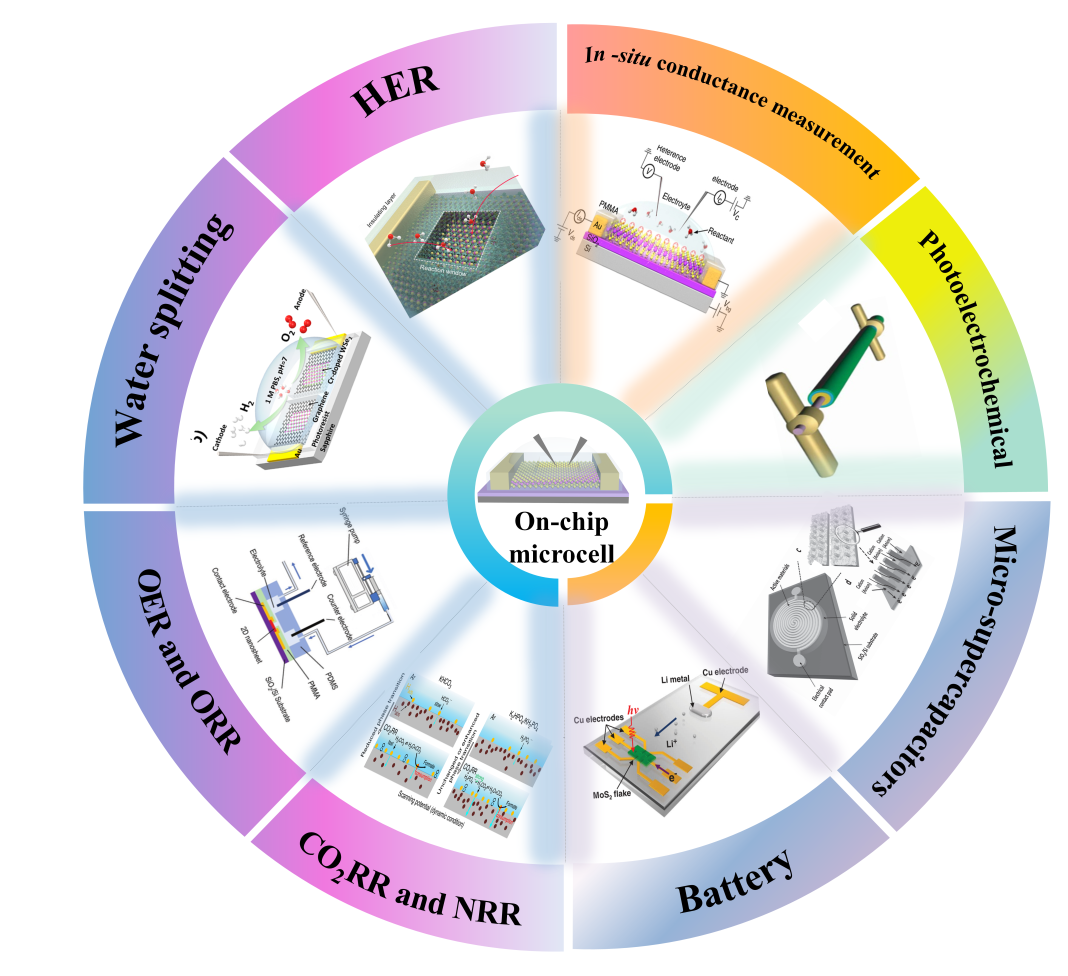
It is crucial to summarize recent research in a timely manner to facilitate continuous progress in this emerging field of study. This review provides a comprehensive summary of the typical construction of micro-devices, along with an in-depth analysis of their essential applications. These innovations are expected to significantly contribute to ongoing research in energy-based materials, particularly regarding the development of individual nanomaterial devices. By simplifying complex practical configurations into streamlined models within micro-/nanodevices, these platforms enable the collection of precise, high-quality signals from individual nanomaterials under complex electrocatalytic conditions. These devices leverage the unique properties of nanomaterials to achieve highly accurate charge transfer and catalytic signaling. This capability is supported by advancements in sophisticated in-situ measurement techniques. By enhancing our understanding of material performance, these innovations contribute significantly to progress in technological development. We highlight recent advancements in nanomaterial-based micro-/nanodevices, focusing on two key areas: energy conversion and energy storage. In the domain of energy conversion, we conduct a comprehensive review of various devices, including photoelectrochemical cells, hydrogen evolution reaction (HER) systems, water-splitting devices, as well as setups for both the oxygen reduction reaction (ORR) and the oxygen evolution reaction (OER). Additionally, we explore systems designed for carbon dioxide reduction reaction (CO2RR), technologies focused on nitrogen reduction reaction (NRR), and bioelectrochemical devices. For the the realm of energy storage, our review focuses on the development of micro-supercapacitors and micro-battery devices. In conclusion, we present a thorough analysis of the current state of on-chip devices and delineate prospective avenues for the advancement of micro- and nanodevices in energy applications.
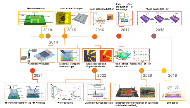
Figure. 1 Timeline for the on-chip microcell in electrocatalysis.[77] Copyright (2010) American Chemical Society; [78] Copyright (2014) Nature Publishing Group; [68, 79] Copyright (2015) American Chemical Society and Nature Publishing Group; [66, 80] Copyright (2016) American Chemical Society and Nature Publishing Group; [67, 81] Copyright (2017) American Chemical Society; [82] Copyright (2018) Nature Publishing Group; [69] Copyright (2019) Nature Publishing Group; [83] Copyright (2020) Nature Publishing Group; [84, 85] Copyright (2022) Wiley-VCH Verlag GmbH & Co and American Chemical Society; [86] Copyright (2024) Nature Publishing Group. |
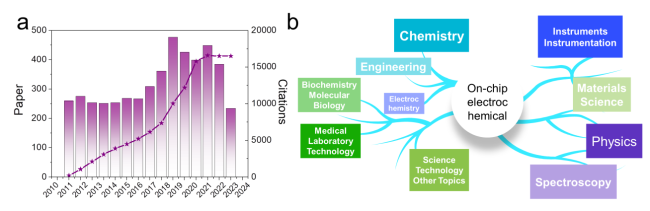
Figure. 2 (a) Annual number of publications by using keyword of “on-chip electrocatalysis” from Web of Science on January 7, 2025. (b) The hot spot in the total circulation. |
2 The preparation of on-chip devices
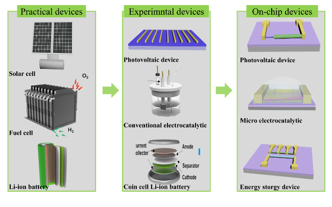
The integration of diverse technologies for energy sector is crucial in the development of specialized devices. These devices must possess the appropriate configurations and structures to effectively carry out their essential functions. This analysis presents a comparison of three widely adopted prototypes in practical applications: solar cells, fuel cells, and lithium-ion (Li-ion) batteries. Each prototype is evaluated in relation to corresponding experimental devices as well as on-chip micro devices designed with delicate configurations. Corresponding diagram of practical configuration, lab testing equipment and on-chip micro-devices are shown in Figure 3. Practical devices with the large size, which should satisfy the requirement industrail manufacture.[87, 88] Experimental devices as the key part to improve the efficient of energy conversion and storage, have simple and delicate components to investigate the mechanism and detail for further optimize.[89, 90] For the micro-device, which is primarily based on top-gated field-effect transistors (FETs) or electric double-layer transistors (EDLT), further miniaturization of the research objects is achieved. This advancement facilitates the investigation of reactions from an electronic perspective, including the modulation of external electric fields, in situ conductance measurement and interface designing for effective charge injection. These on-chip devices are engineered for the energy sector, providing substantial and dependable physical functionalities. It holds significant potential for uncovering novel phenomena and enhancing our understanding of electrochemical fundamentals at the nanoscale.
2.1 Photovoltalic devices
As early as 2007, Lieber et al. conducted a study on the development of an on-chip solar cell utilizing a single p-i-n silicon nanowire. This innovative approach represents a significant advancement in solar energy technology.[91] The highly doped silicon substrates include a 100 nm thermal oxide layer and a 200 nm silicon nitride (SiNx) layer as the foundational components. Chromium (Cr) pads were utilized to firmly position the nanowires. The final device is constructed by applying metal electrode to both the p-core and n-shell of the Si nanowires. Initially, the p-core was selectively exposed in designated areas through the process of electron beam lithography (EBL). Subsequently, silicon oxide (SiO2) and the shells of the silicon nanowires were etched away using buffered hydrofluoric acid (HF) and potassium hydroxide (KOH), respectively. In the concluding step, titanium (Ti) in a thickness of 3 nm and palladium (Pd) in a thickness of 500 nm were deposited to form contacts on the Si nanowires using EBL and thermal evaporation techniques.
2.2 Energy conversion devices
As the on-chip electrocatalytic devices, the fabricated process as follows: First, the catalysis is direct growth or mechanical exfoliate placed onto a SiO2/Si wafer, The substrate underwent spin-coating with PMMA at a speed of 4, 000 rpm for 40 seconds, followed by a baking process at 60 °C for 5 minutes. Subsequently, EBL was utilized to expose the designated electrode area. Following this, Cr/Au electrodes (10 nm/50 nm) were deposited using thermal evaporation. The final device was then immersed in acetone to remove the residual PMMA, followed by isopropanol, and was subsequently dried with nitrogen gas.
2.3 Energy storage devices
Physical micro-electrical devices are fabricated through photolithography and electron-beam lithography[92, 93] combined with metal deposition methods.[94, 95] The integration of nanomaterials into a circuitry framework establishes the fundamental unit for electrical measurement. An exemplary approach by the Mai group focuses on understanding the transport characteristics of Li+ and Na+ within nanoscale battery electrodes. This investigation involves the recording of conductance across various regions of the nanowire during charge and discharge cycles by designing contacts site on a single nanowire electrode. Once nanomaterials are incorporated into a circuitry framework, the fundamental unit for charge transfer measurement is established. An exemplary approach by the Mai group focuses on understanding the transport characteristics of Li and Na ions within nanoscale battery electrodes. This investigation involves the design of multiple contact electrodes on a nanowire, which facilitates the collecting of multiple signals across various regions of the nanowire during charge and discharge cycles, thereby yielding valuable insights. The device comprises a single H2V3O8 nanowire as the cathode and a highly oriented pyrolytic graphite (HOPG) flake as the anode. The invention of different contacts point enables simultaneous electrical transport tests on distinct segments of the single nanowire, enhancing the understanding of both electron and ion transport mechanisms. To comprehensively investigate ion transport for the nanowire, different position and corresponding mechanism are tested and analysis, allowing for an in-depth analysis of its electrical transport properties.
As mentioned above, photovoltaic devices, energy conversion devices, and energy storage devices each require distinct circuits and fabrication processes tailored to their specific applications. A common methodology for fabricating these three types of devices includes traditional optical and electron-beam lithography, as well as metal deposition techniques. Photovoltaic devices and energy storage devices typically employ physical circuitry, which involves the integration of nanowires for fundamental electrical signal testing. In contrast, the fabrication of energy conversion devices, characterized by a three-dimensional architecture, is considerably more complex. For instance, the use of insulating layers such as PMMA, SU-8, and photoresist is crucial for obtaining precise signals through exposure catalysis. Additionally, the diameters of counter electrodes (CE) and reference electrodes (RE) must be maintained at small sizes to ensure their complete immersion in the testing droplet. As this electrochemical measurement technique is still evolving, several challenges within the fabrication process require further optimization and attention. One notable concern is the use of Ag/AgCl as a micro reference electrode. It is important to recognize that AgCl is susceptible to decomposition when exposed to light, which can lead to unstable potential and impede the progress of electrochemical measurements. Continuous assessment of the testing system's reliability is necessary, utilizing the Pt film as the working electrode for accurate calibration against the commercial platinum reference. Additionally, the electric and catalytic signals generated by microscopic catalysts typically operate at the nanoampere (nA) level. Consequently, maintaining a stable testing environment is imperative to mitigate the influence of external disturbances, including vibrations, light fluctuations, and electromagnetic interference. Meeting the demands of in-situ characterization requires that these micro devices be designed and fabricated with a complex, objective-oriented, and tunable configuration. The chip configuration is determined by a comprehensive understanding of both practical and experimental devices, in addition to the principles of physical circuitry.
3 Energy conversion
3.1 Hydrogen evolution reaction (HER) device
Large-scale electrical energy storage is widely acknowledged as one of the most significant challenges in the transition from fossil fuels to clean, sustainable energy sources. The electrochemic conversion of inert molecules—such as H2O, CO2, and N2—into valuable chemicals, including hydrogen, hydrocarbons, oxygenates, and ammonia, presents an efficient approach to energy storage.[97-99] Hydrogen is frequently recognized as one of the cleanest energy sources of the 21st century, owing to its abundance, renewability, and high energy density.29, 100-102 Presently, water electrolysis stands out as the most efficient and practical method for hydrogen production. In this process, the role of electrocatalysts is vital, as they significantly enhance both the rate and efficiency of hydrogen generation.[103]
The growing interest in electrocatalysis is driven by the need to explore underlying mechanisms and optimize performance. While macro-scale energy devices are useful for validating material efficiency and stability in practical applications, they are less effective in revealing fundamental principles, particularly for micro- and nanoscale materials. Consequently, micro /nanodevices are becoming increasingly important for advancing our understanding of these processes and are expected to lead to significant breakthroughs.
3.1.1 Identification of active sites
Energy-based on-chip micro-devices have progressed from their origins in physical device platforms to become unique and significant tools for research. Their advancement underscores their importance in various scientific applications. These devices function as simplified models, facilitating high-precision measurements and the validation of fundamental principles. In on-chip micro-/nanodevices, the active region is critical, as the primary goal is to accurately capture and analyze signals from specific materials and localized regions, particularly at the single-nanomaterial level. Electrochemically inert materials, such as PMMA, are frequently utilized as cover layers to form various exposure configurations, enabling precise characterization of reaction kinetics at targeted sites. These advanced on-chip devices are capable of achieving precise and targeted measurements of catalysis sites through the meticulous design of nanocatalysts.
(Basal and edge) MoS2 has been recognized as a highly effective catalyst for the HER. This recognition is largely attributed to its low energy barrier and cost-effectiveness, making it a valuable material for advancements in catalysis. Research findings indicate that the catalytic performance of MoS2 is significantly influenced by its edge sites. However, conventional macro-scale electrochemical systems face challenges in conclusively identifying these active sites. By utilizing an individual MoS2 nanosheet within an on-chip device, this limitation can be overcome, providing a more effective platform for directly demonstrating and studying the catalytic activity at the nanoscale. Lou's research group conducted a comprehensive study on the HER activity of 2H and 1T'-MoS2 monolayers, as detailed in Figures 4a-g. The research team utilized an on-chip microcell to conduct a detailed investigation into the performance of the basal plane and edge sites. The findings provided compelling evidence that edge sites demonstrate significantly enhanced catalytic activity when compared to the in-plane regions, irrespective of the presence of 1T'-MoS2 or 2H-MoS2 phases. Furthermore, the investigation revealed that the in-plane region of 1T'-MoS2 exhibited superior activity relative to that of 2H-MoS2.[64] This precise, quantitative local measurement method offers an effective approach for assessing the catalytic activity of nanomaterials across large sample sets. Chhowalla's research team conducted a comprehensive investigation into the impact of vacancies on the inert MoS2 basal plane. Additionally, they evaluated the activity of individual samples with varying vacancy concentrations. Their study demonstrated that catalytic activity increases proportionally with the concentration of vacancies. (Figure 4h1-h4) The efficacy of electron transfer across various surfaces is a crucial factor influencing catalytic activity. Research indicates that the 2H-MoS2 basal plane can attain performance levels comparable to those of 1T-MoS2 by effectively monitoring interface contact.[80] In addition to flat individual nanosheets, Prasad V. Sarma et al. synthesized vertically oriented dislocation lines interconnected with helical WS2 domains, systematically investigating how these dislocation lines and edge sites influence catalytic performance for hydrogen evolution using microelectrochemical techniques (Figure 4i1-i5). The dislocation lines function as connectors for multiple active edge sites oriented vertically, thereby enhancing vertical charge transfer, contributing to the improved performance of WS2.[104] Furthermore, the activity of edge sites in WTe2 and PtSe2 has also
been demonstrated using on-chip microcells.105 106 (Figure 4j1-j4)
been demonstrated using on-chip microcells.105 106 (Figure 4j1-j4)
(phase and layer) The phases and the number of layers greatly affect the catalytic properties and conductivity of two-dimensional materials. For instance, as shown in Figures 5a and 5b, Zhang fabricated three different phase compositions of MoS2: 2H-2H and 1T-1T homo-phases, as well as a 2H-1T hetero-phase. Especially, the 2H-1T hetero-phase has undergone testing to evaluate its high performance capabilities. This enhancement is attributed to the superior charge transport capabilities of the metallic 1T phase in comparison to the electrochemically inert 2H phase.[82] Although the 2H is relatively stable, the 1T displays metallic behavior and demonstrates enhanced activity for the HER. Additionally, the micro-device with tiny and precise windows offers a systematic approach to exploring the one-dimensional (1D) catalysts regarding the boundary length-dependent HER. Conventional bulk measurements are inadequate for accurately examining these 1D heterophase regions in relation to HER. Lee et al. conducted a study that analyzes the junction line between the 2H and 1T' phases of MoTe2. Their research provides valuable insights into the structural properties of this material. Their research demonstrated significant charge accumulation, confirmed through Kelvin probe force microscopy (KPFM). The findings underscored the unique covalent characteristics of the heterophase boundary, which significantly contributed to the enhanced HER performance of MoTe2. This study provides valuable microscopic insights that deepen our understanding of the material's exceptional catalytic properties.[107] Jiao et al. examined how the thickness of PtSe2 influences HER activity using on-chip microcells (Figures 5d-f).
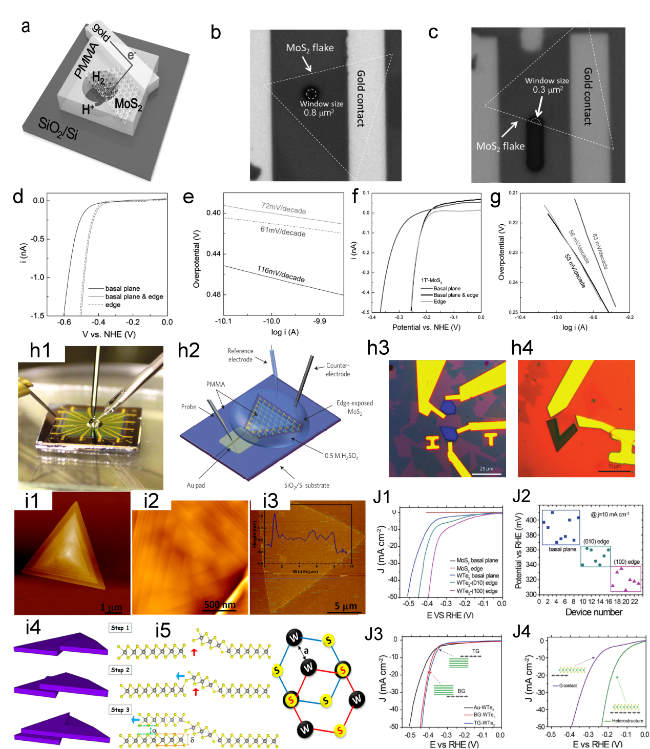
Figure 4. (a) Schematic of the on-chip setup. Optical image of a MoS2 showing the (b) basal and (c) edge planes. (d) LSV and (e) Tafel plots of the MoS2 with basal plane and edge, the electrolyte was argon-purged in 0.5 M H2SO4 and scan rate was set at 10 mV s−1. (f) LSV and (g) Tafel curves of monolayer 1T′-MoS2 basal plane, and edge in HER.[64] Copyright 2017, Wiley-VCH Verlag GmbH & Co. (h1) Photograph of the electrochemical microcell. (h2) Schematic of the on-chip electrocatalytic. Optical microscope images of single-layer MoS2 with (h3) the basal and (h4) edge exposed.[80] Copyright 2016, Nature Publishing Group. (i1, i2) AFM of spiral WS2 domains and (i3) corresponding height of monolayer WS2. (i4) Schematic of the spiral domain growth modes. (i5) Schematic of the atomic arrangement in spiral WS2.[104] Copyright 2019, American Chemical Society. (j1) LSV of MoS2 and WTe2 with different exposed area, the overpotential of (100), (010) edge and basal plane is 320 ± 10 mV, 350 ± 10 mV and 390 ± 20 mV respectively at 10 mA cm−2. (j2) Summary of the overpotentials for WTe2 with different exposed sites. (j3) LSV of WTe2 with basal plane. (j4) LSV of MoS2 with a graphene contact, as well as from the MoS2/graphene heterostructure.[105] Copyright 2018, Wiley-VCH Verlag GmbH & Co. |
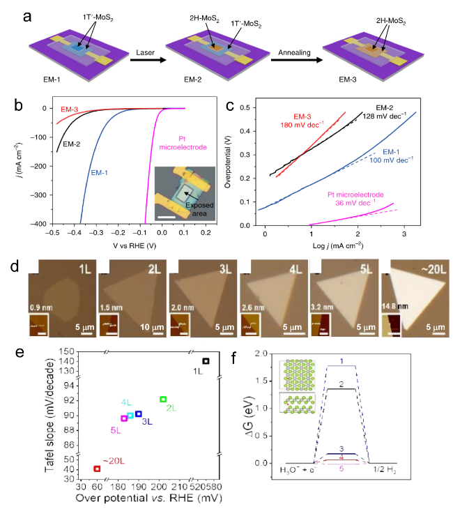
Figure 5. The diagram of fabrication process. (b) The LSV for EM-1, EM-2, and EM-3, with an inset image EM-1, the overpotential of EM-1 and EM-2 is 165 mV and 200 mV, respectively. Scale bar, 20 μm (c) Tafel plots corresponding the (b).[82] Copyright 2018, Nature Publishing Group. (d) Optical images of CVT-grown PtSe2 flakes ranging from 1 to 20 layers, insets show the corresponding AFM images. (the same height scale for AFM images, the scale bar of first is 1 μm, others is 0.5 μm) (e) LSV and Tafel slops for the HER. (f) ΔGH diagram for HER of different layer PtSe2.[106] Copyright 2019, Wiley-VCH Verlag GmbH & Co. |
Recent work on 2D PtSe2 with varying layer thicknesses has led to its successful synthesis and thorough evaluation regarding its HER performance.[106] The findings indicate that thicker layers of PtSe2 demonstrate significantly enhanced HER activity. Conversely, for most bulk or few-layer TMDCs, the weak interlayer electron coupling adversely impacts vertical conduction, resulting in diminished HER performance. These insights underline the importance of layer thickness in optimizing the performance of materials for energy applications.
(Catalytic window) The development of the on-chip microcell significantly enhances our understanding of individual nanowires and nanosheets, particularly in relation to conductance challenges within the reaction windows of non-metallic catalysts. Xia et al. utilized in-situ technology to concurrently collect electrical and electrochemical signals, with the objective of examining the conductance challenges associated with window size.[108] Their research highlighted the superior performance of a fully open MoS2 window, which allows for complete exposure of the catalyst channel, thereby facilitating more effective charge transfer. To address the conductance issues identified, they devised a vertical microcell strategy that effectively mitigates these challenges and improves measurement reproducibility. This work has provided valuable supplementary instruction for ensuring the reliability of micro-device testing and has established a solid foundation for future research in on-chip technologies.
3.1.2 Methodology for enhancing HER performance
Numerous strategies exist to optimize catalytic performance, such as activating the inert basal plane and enhancing conductivity.[109-111] Various complex and dynamic factors significantly influence catalytic activity in the electrocatalysis process. Conventional methods of electrocatalytic testing often face challenges in isolating individual variables, which can complicate the assessment of specific influences. On-chip electrocatalytic microdevices present a solution by allowing designs that concentrate on a single structural factor. This approach minimizes interference from other variables and enables precise monitoring of changes in active sites.
Grain boundaries (GBs) and sulfur (S) vacancies are prevalent line defects in transition metal dichalcogenide (TMD). Utilizing microcells, the performance of individual GBs can be accurately detected. He et al. have achieved the successful synthesis of a wafer-level, atomically thin TMD. This material exhibits notable HER performance, attributed to the presence of a significant number of GBs. Electrochemical testing of the base surface with high-density GBs demonstrated excellent hydrogen production (Figure 6a1-a5). [112]Moreover, the impact of vacancies on catalytic performance can also be investigated using microcells. Manish Chhowalla's group bombarded CVD-grown monolayer MoS2 with He ions to create sulfur vacancies in the basal surface and employed high-resolution spherical aberration imaging to precisely determine the concentration of single-atom sulfur vacancies. The HER activity associated with these vacancies was quantitatively characterized by combining the MoS2 window with a defined exposure area using selective exposure technology. They found that as the concentration of sulfur vacancies increased, the hydrogen production rate per active site, measured by turnover frequency (TOF), also increased, indicating that a high concentration of sulfur vacancies can serve as effective active sites. [112]
Doping: Doping is a widely recognized technique employed to enhance catalytic performance. Previous research has primarily concentrated on doping the basal plane, yet it is important to recognize that doping at the edge active sites can also induce significant structural and activity changes. A comprehensive understanding of the effects that edge-active dopants have on structure is essential for elucidating the mechanisms underlying catalytic processes. Ye et al. conducted a study on P doping in MoS2, investigating the influence of doping on edge sites through the use of an on-chip electrocatalytic microcell, which enabled spatially resolved catalytic measurements.[113] Their in-situ transport measurements confirmed that the observed high performance is attributable to the activity site of the P-doped MoS2 rather than to conductance factors. (Figure 6b1-b7) Furthermore, the incorporation of heteroatoms of varying sizes often leads to the formation of vacancies. However, systematic analyses of the synergistic effects of heteroatoms and vacancies remain scarce. Liu et al. addressed this gap by employing a chemical vapor deposition (CVD) method to synthesize different defect configurations by varying the concentration of V doping in the inert face.[116] Their study facilitates a detailed examination of the basal plane under different doping conditions and sulfur vacancy configurations through precise selective exposure techniques. Through density functional theory (DFT) calculations and an analysis of hydrogen adsorption free energy (∆GH*), the No. 9 defect, referred to as Sub3V doping, has been validated and is demonstrating significant high performance, which is characterized by a relatively high abundance of sulfur vacancies. This research systematically summarizes the potential of point defect-derived MoS2 electrocatalysts, offering valuable insights for the design of high-performance catalytic materials.
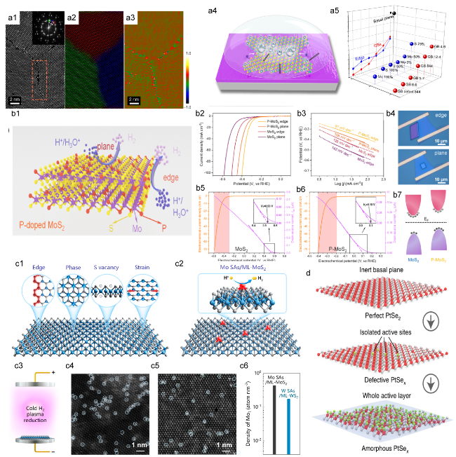
Figure 6. (a1) The HAADF STEM image of the GBs between three MoS2 grains, the inset on the left shows the Fourier transform. (a2) The composite color-coded inverse fast Fourier transform (IFFT) image. (a3) illustrates the Geometrical Phase Analysis (GPA) routine.[112] (b1) Schematic of HER process on P-MoS2 nanosheets. (b2) and (b3) show the LSV and Tafel plots for the MoS2 and P-MoS2, The edge sites show an onset potential (η10) of 297 mV and a Tafel slope of 97 mV dec−1 for HER, exceeding those of the basal plane with 328 mV and 108 mV dec−1. (b4) Optical images of edge and basal plane on a P-MoS2. (b5) and (b6) display the electrochemical and electronic signals of a MoS2 and P-MoS2 during the HER. (b7) Illustrates the electronic structure of P-MoS2, aligning the Fermi levels.[113] Copyright 2017, American Chemical Society. (c1) Schematic of the active sites of MoS2. (c2) Schematic of Mo ML-MoS2. (c3) Details the synthesis of metal SAs on a ML-MoS2. HAADF-STEM images in panels (c4) and (c5) depict Mo SAs on ML-MoS2 and tungsten SAs on monolayer WS2 samples, respectively. (c6) statistical results on the density of Mo and W SAs on 2D monolayers.[114] Copyright 2020, American Chemical Society. (d) Schematic of the amorphous PtSex surface, perfect PtSe2 and defective PtSex.[115] Copyright 2022, Nature Publishing Group. |
Design single atom: Metal doping has also been explored and validated through microcell measurements.[113] Liu and colleagues have achieved the successful synthesis of molybdenum (Mo) single-atom doped MoS2 utilizing the hydrogen plasma reduction method.(Figure 6c1-c6). Single-flake microcell measurements demonstrated that this catalyst exhibited exceptional intrinsic activity. The authors attributed the improved performance to increased bond strength resulting from hybridization, which facilitates
rapid hydrogen adsorption and desorption kinetics, thereby enhancing HER activity.[114] To achieve optimal electrocatalytic activity and stability, emerging trends in catalysis are increasingly focusing on the implementation of single-atom noble metal catalysts arranged in a monolayer configuration. This approach allows for the reconfiguration of nearly all atoms to enhance performance. He et al. have recently presented their findings on a wafer-sized amorphous PtSex film, produced through the ion etching of low-temperature argon plasma. Their investigation utilizing a micro-electrochemical cell demonstrated that this amorphous PtSex film, characterized by high atom utilization and a robust single-layer structure, exhibits exceptional catalytic performance that is comparable to that of commercial Pt. [115]
rapid hydrogen adsorption and desorption kinetics, thereby enhancing HER activity.[114] To achieve optimal electrocatalytic activity and stability, emerging trends in catalysis are increasingly focusing on the implementation of single-atom noble metal catalysts arranged in a monolayer configuration. This approach allows for the reconfiguration of nearly all atoms to enhance performance. He et al. have recently presented their findings on a wafer-sized amorphous PtSex film, produced through the ion etching of low-temperature argon plasma. Their investigation utilizing a micro-electrochemical cell demonstrated that this amorphous PtSex film, characterized by high atom utilization and a robust single-layer structure, exhibits exceptional catalytic performance that is comparable to that of commercial Pt. [115]
Construct Heterostructure: Heterostructures are defined as the interface regions formed by the contact of two distinct semiconductors. The interface consists of diverse band structures in 2D materials, highlighting their unique electrical transport properties. This variability underscores the potential applications of these materials in various technological advancements. The investigation of micro-region electrocatalysis within specific areas of a heterojunction significantly enhances our understanding of charge transfer and interface dynamics during catalytic processes. For example, research conducted by Cha et al. demonstrated a notable improvement in the HER activity of MoS2 through the introduction of a graphene support layer, resulting in the formation of a MoS2/graphene heterostructure. (Figure 6d).[105] Similarly, Zhou et al. have demonstrated that the heterostructure interface formed by MoS2 and WTe2 significantly enhances charge transfer efficiency, thereby improving the HER activity.[117]
Molecule/ligand-linked inorganic solids (MLIS) serve as effective tools for enhancing a range of electrocatalytic processes and have been extensively researched in the field. A critical area of inquiry focuses on understanding which mechanism predominates in the operation of MLIS. Traditional electrochemical methods have limitations, as isolating and quantifying the distinct contributions of these effects to catalytic activity can be quite challenging. The electrical transport spectroscopy (ETS) provides a promising approach for monitoring the conductance of single catalysis, thereby facilitating quantitative fundamental research. Notably, the external electric field engineering of these microdevices allows for the electronic simulation of charge doping in molecular-linked catalysts, enabling a clearer distinction between the various contributions to catalytic performance. In their study, Liu et al. employed typical MoS2 and the n-type dopant methylene blue (MB) molecules to explore the promotional influence on HER performance.[118] In-situ conductance measurements have provided insights into the charge injection from molecular buffers (MB) to MoS2. These findings quantitatively demonstrate that charge injection is not the primary factor contributing to the high performance of the HER. Instead, the enhancement of HER activity is primarily attributed to proton enrichment in the vicinity of MoS2, a process facilitated by the nucleophilic groups present in MB. This conclusion is further corroborated by on-chip electrochemical impedance measurements.
Electric Field Modulation: Micro-devices are engineered to investigate the fundamental physical properties of semiconductor materials. Field-effect transistors (FETs) leverage an insulating layer in conjunction with an external electric field, enabling precise electron injection from metal microelectrodes. This approach facilitates a deeper understanding of the behavior and characteristics of these materials, which is essential for advancing semiconductor technology. Moreover, this modulation enables the study of electrocatalytic processes under a back-gated electric field. Early work by Cummins et al. demonstrated the ability to tune the HER performance of MoOx/MoS2 core-shell nanowires using electric-field tuning
(Figure 7a-c).[119]
(Figure 7a-c).[119]
Recent studies have demonstrated that the application of external gating can significantly influence the state of electrons, the behavior of charged ions, and d-states. Notably, research conducted by the Mai Group has elucidated the effects of electric fields on the physical properties of MoS2 during electrochemical processes. This work contributes valuable insights into the complex interactions within these systems. (Figure 7d).[120] Their findings indicated that a positive gate voltage enhanced the MoS2 nanosheet's performance, attributed to increased channel conductance. The observed improvement can be attributed to the Fermi level moving closer to the bottom of the conduction band in response to the application of a positive gate voltage. This shift results in a significant reduction of the energy barrier, which in turn enhances conductivity. Furthermore, similar conductivity modulation influenced by the electric field has been documented in other research studies, thereby reinforcing these results. [121-123] Furthermore, VSe2 nanosheets demonstrated field-effect-tuned performance in the HER, exhibiting characteristics of a metallic material that remains unaffected by electric fields. This study effectively isolated the impacts of ions and electrons, revealing that concentrated hydrogen ions significantly enhance the dynamics of adsorption. (Figure 7e-f).[81] Frisbie et al. successfully modulated the ΔGH* and enhanced the performance of the HER by applying increased back-gate voltages. The observations indicated no significant variation in the resistance of MoS2, thereby eliminating the potential influence of conductivity effects on the results obtained. DFT calculations have elucidated that the application of an electric field induces modifications in the d-states of Mo. Importantly, the existence of sulfur vacancies has been recognized as a critical determinant in the augmentation of Mo-H binding energy, as illustrated in Figure 7g-h.[67] Furthermore, it was observed that the ΔGH* for electron-enriched WSe2 is notably lower compared to that for hole-enriched WSe2 when modulated by an electric field as confirmed by Dong et al.[124] Zhai et al. demonstrated that the external field can modulate charge transfer and enhance Mo-H bonding in the CoPc/MoS2 heterostructure. [125]
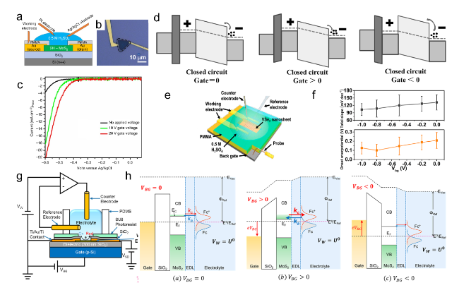
Figure 7. (a) Schematic of the gate-modulation electrochemical device. (b) Optical images of 2H-MoS2 with Au pads. (c) LSV of gate-dependent HER measurements, the green and red curves show the improvement in electrocatalytic activity after applying a positive gate voltage of 10 and 20 V, respectively.[119] (d) Energy band diagrams of the MoS2 device at different gate bias.[120] Copyright 2017, Wiley-VCH Verlag GmbH & Co. (e) Schematic of the HER device under back gate voltages. (f) Statistic-based influence of the back gate on the onset overpotential and Tafel slope.[81] Copyright 2017, American Chemical Society. (g) Schematic of a back-gated electrochemical cell. (h) Energy band diagrams of the MoS2 at various back-gate biases.[67] Copyright 2017, American Chemical Society. |
Oriented electric fields (OEF) have the capacity to align protons and subsequently modify the charge distribution within the double layer. This alteration in the interface potential can significantly enhance reaction activity by reducing the reaction barrier. Most research to date has concentrated on the behavior of entire nanosheets, while the properties of the edges of 2D materials have received considerably less attention. To address this oversight, Ya-Ping Hsieh and colleagues have reported findings on the enhancement of electrochemical processes at the edges of 2D materials driven by OEFs. The team successfully engineered localized operational electric fields (OEFs) through the construction of a heterojunction nanoribbon composed of fluorographene, graphene, and MoS2. This achievement has been validated via simulations and spatially resolved spectroscopy. Furthermore, the development of an on-chip device, complemented by impedance measurements, facilitates precise evaluation of the edge/electrolyte interface. These assessments have demonstrated a significant enhancement in the heterogeneous charge transfer rate between the edge and the electrolyte. This work underscore the potential of OEFs in advancing the understanding and application of edge-based electrochemistry in 2D materials.[126]
Single-atom catalysts (SACs) have attained considerable attention in the scientific community for their potential to enhance catalytic processes. However, there is still a lack of exploration regarding the enhanced functionalities of single-atom catalysis, particularly in the context of electric field modulation. SACs have the capability to generate internal local electric fields, referred to as the "tip effect", in specific orientations dictated by their fixed electronic structures. These electric fields can significantly influence both the activation of reactants and the distribution of ions within the electrolyte.[127-129] Recent research by Pan et al. has demonstrate the existence of oriented external electric fields (OEEFs) for the single-atom catalysts anchored on 2D materials, which lead to the high performance through systematically optimized.[130] Specifically, utilizing a microcell platform, they found that Pt SAs-MoS2 exhibited substantial enhancements in catalytic activity under positive OEEFs. In comparison, Co SAs-WSe2 demonstrated a significantly improved activity for the OER. In real-time measurement, coupled with EIS and DFT calculations, have revealed an “onsite electrostatic polarization” mechanism. This mechanism involves a vertical electric field generated by single-atom sites, which polarizes metal atoms, adsorbates, and intermediates. This polarization leads to substantial modifications in charge state and kinetics pathways during electrochemical process. The modulation of various single atoms through OEEFs has demonstrated an effective approach to enhancing catalytic performance. Furthermore, this method is a proper model for enzyme-mimicking artificial modulation, thereby promoting a deeper understanding of bio-electrochemical processes in general.
Thermal Modulation: In addition to the electric field effect, the catalytic performance under thermal conditions can be effectively assessed using on-chip devices. Qu et al. have successfully developed an ML MoS2 micro-reactor aimed at examining the direct thermal enhancements in HER applications. The applying of thermal energy identified facilitate charge transfer both within the atomic structure of the MoS2 monolayer and the interface of solid-liquid catalysis. This leads to a notable improvement in HER activity.[131] These findings indicate that the utilization of micro devices presents a valuable opportunity to investigate thermal effects on two-dimensional monolayers and may make the foundation for the advancement of high performance electrocatalysts.
3.2 In situ measurement on-chip device
The dynamics at the interface of electrocatalytic reactions are inherently complex and serve a vital role in achieving efficient energy utilization. Real-time, in situ regulating of the interface between the solid and liquid in the catalytic process significantly enhances our understanding of the surfaces and interfaces involved in electrocatalysis, which is critical for the advancement of future catalyst development. The emerging technology of on-chip electrical transport spectroscopy (ETS), which employs a field-effect transistor (FET)-analog structure, enables comprehensive in situ monitoring of the electronic properties of electrode materials. By providing information through diverse electrical transport signals, ETS allows for the measurement of varying interfacial states across a wide range of electrode materials. Its sensitivity, specificity, and quantification capabilities offer a robust experimental foundation for studying electrochemical mechanisms under operando conditions.
Ding group developed an innovative in situ ETS method to directly examine the electrochemical interfaces of platinum nanowires (Pt NWs). This technique employs dual-channel measurements—both electrochemical and electrotransport—utilizing advanced micro-devices (refer to Figure 8g-i).[68] The results demonstrate that the conductance of Pt NWs exhibits both sensitivity and selectivity to electrochemical surface states. The researchers successfully identified distinct redox regions, including those related to the HER, hydrogen adsorption/desorption (Hupd), double layer (DL), surface oxide formation/reduction (Oupd), and OER. This differentiation is clearly depicted in the IG-VG and GSD-VG curves. Additionally, the ETS method was employed to investigate various electrocatalytic reactions, further establishing its versatility and reliability. The emerging on-chip measurement represents a powerful tool that offers distinctive and varied insights into the electrocatalytic process. This advancement is significant for understanding and enhancing electrocatalytic systems.
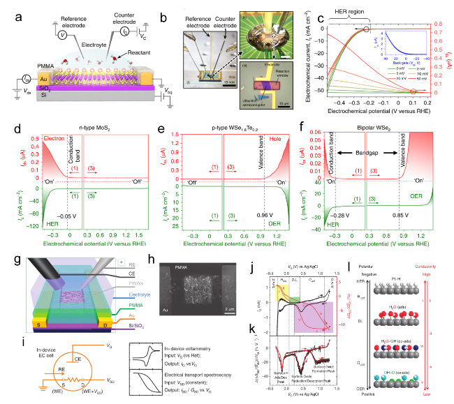
Figure 8. (a) Schematic of the microcell-based in situ electronic/electrochemical measurement. (b) Optical image of the microcell. (c) Typical electrochemical (y axis in black) and electronic (y axis in red) signals of single-layer WS2 during the HER at different bias potentials. Self-gating phenomenon of (d) n-type MoS2, (e) p-type WSe1.8Te0.2, and (f) bipolar WSe2, typically, n-type MoS2 is turned on at a negative electrochemical potential and only delivers the HER, p-type WSe1.8Te0.2 is turned on at a positive electrochemical potential and only delivers the OER, bipolar WSe2 is turned on at both negative and positive electrochemical.[69] Copyright 2019, Nature Publishing Group. (g) Schematic of the Pt NW device. (h) SEM image of the device cell. (i) Schematic of CV and ETS for in situ monitoring of the electrochemical interfaces. (j) The IG-VG and normalized GSD-VG characteristics of a typical Pt NW device, IG-VG resembles the typical CV characteristic of a polycrystalline Pt surface, containing redox regions of HER, H adsorption/desorption region (Hupd), double layer (DL) region, surface oxide formation/reduction region (Oupd) and OER. (k) The differentiated ETS curve illustrates spectral peak characteristics. (l) Schematic of various Pt surface conditions along with the sweeping electrochemical potentials (left black axis) and the corresponding changes in conductivity.[68] |
The HER catalyzed by platinum typically demonstrates diminished kinetics in alkaline electrolytes, which indicate complex kinetics process. In alkaline environments, the effect of alkali metal cations contribute to a more complex electrode-electrolyte interface (platinum-water) compared to that found in acidic media. While there is a consistent observation that lithium ions (Li+) enhance HER activity on platinum electrodes relative to larger alkali metal cations, a comprehensive understanding of this phenomenon remains a subject of active discussion. The performance of the HER consistently exhibits distinct characteristics in various alkaline environments. The role of cations in the electrocatalytic process is particularly significant. Therefore, a thorough investigation of the catalytic processes at the electrode-electrolyte interface is essential for deepening our understanding of the mechanisms that operate under alkaline conditions. Shah et al. utilize a distinctive technique called ETS to directly examine platinum surface adsorbates across varying potentials. Additionally, they employ EIS to analyze the solid liquid interface within the electric double layer (EDL) and assess the charge-transfer resistance (Rct) at the solid-liquid interface.[132] Their findings indicate that HER activity in alkaline media is contingent upon the specific alkali metal cation present, with the activity ranking as follows: Li+ > Na+ > K+. This study employs a combination of experimental and theoretical methods to elucidate the intricate role of alkali metal cations. The findings indicate that these cations have an indirect influence on the presence of hydroxyl species (−OHad). This increased coverage of hydroxyl species, particularly with smaller cations, is beneficial for enhancing HER activity. Notably, the research reveals that Li+ cations exhibit a lower destabilizing effect on OHad adsorption compared to Na+ and K+. This allows for greater retention of hydroxyl species, facilitating the kinetics of the Volmer step and subsequently enhancing catalytic performance in alkaline electrolytes. The conclusions derived from the EIS analysis indicate that the increased sheet resistance is associated with a higher concentration of OHad present on the surface in comparison to Na+ and K. The comprehensive findings from this study provide critical insights into the manner in which alkali metal cations influence HER kinetics in alkaline media.
Adsorbed hydrogen (Had) serves as an essential intermediate in the HER kinetic, and it interacts with various active sites on Pt.[86] Understanding these interactions is essential for the development of advanced nanocatalysts.[133, 134] Identifying the specific active sites related to Had and their underlying mechanisms is vital for informed catalyst design. A study conducted by Huang et al. examined Had on Pt nanowires and identified two distinct peaks: one at 0.20 V versus the reversible hydrogen electrode (RHE), associated with the (111) and (100) facets, and another at 0.038 V RHE, which corresponds to the edge sites.[86] Their research indicates that hydrogen adsorption at edge sites aligns with the onset of the HER, as demonstrated through electrochemical assessments, including electrochemical temperature scans (ETS) and cyclic voltammetry (CV). Significantly, the ETS evaluations in alkaline media reveal that Had on edge sites is decease significantly, leading to slower overall kinetics of the HER. These findings provide direct evidence and valuable insights into the relationship between electrocatalytic performance and the various active sites.
In field-effect transistor (FET) testing, applying an external electric field enhances free carrier mobility, resulting in the typical "on" state of semiconductor materials. Beyond the traditional dielectric layer that exerts field pressure through metal electrodes, research has increasingly focused on forming an electric double layer on ion surfaces by applying voltage, enabling electric field control.[135-139] This electric double layer induces significant capacitance at the interface, facilitating ultrahigh carrier accumulation and effective conductance modulation in semiconducting catalysts. However, systematic studies on the exceptional catalytic performance of semiconductor materials with low conductivity and the potential regulation of carriers during electrocatalytic processes remain limited. He et al. employed on-chip microcells to demonstrate that the “take-on” behavior of semiconductors is linked to the progression of electrocatalysis, a phenomenon termed self-gating.[69](Figure 8a-f). MoS2 is a well-established n-type semiconductor that shows enhanced conductivity at negative electrochemical potentials, thereby facilitating reactions at these potentials, particularly the HER. Conversely, at positive electrochemical potentials, it enters a low-conductance state, inhibiting anodic reactions. In contrast, the P-type semiconductor WSe₁.₈Te₀.2 activates at positive potentials, facilitating anodic reactions. The bipolar WSe2 demonstrated notable activity across both positive and negative potentials, effectively enabling HER and OER. The advancement of in-situ monitoring technology enables the provision of multidimensional information regarding electrochemical surface states. This capability enhances our ability to analyze the reaction mechanisms that occur within complex environments. This innovative methodology addresses the limitations associated with conventional electrocatalytic measurements and enhances our comprehension of electrocatalytic surfaces and interfaces, which is essential for the development of next-generation catalysts. In the realm of electrocatalytic reactions, the detection and characterization of transient intermediates hold paramount importance for elucidating the mechanisms underlying these processes. In addition to on-chip ETS, various in situ characterization techniques offer valuable insights into catalytic reactions and their interactions with reactants under operational conditions.[140-144] For example, Ren et al. employed tip-enhanced Raman spectroscopy (TERS) to explore the electric and electrochemical properties of a Pd/Au(111) bimetallic model. This advanced technique facilitates the differentiation of molecular vibrations at the nanoscale, thereby enhancing our understanding of surface sites in greater detail.[140] Edward H. Sargent and colleagues have probed the oxidation kinetics of NiCoFeP oxyhydroxides employing in situ soft X-ray absorption spectroscopy (sXAS).[142] Research conducted by Héctor D. Abruña and colleagues has revealed a significant enhancement in photocatalytic efficiency for water splitting. This improvement is attributed to the irreversible surface reordering of n-doped SrTiO3 (001) that occurs as a result of the electrochemical "training" process.[141] Operando high-energy X-ray reflectivity measurements confirmed that this training process leads to irreversible changes in surface structure. Moreover, recent developments in in situ X-ray photoelectron spectroscopy (XPS) and in situ Raman measurements have been successfully implemented under continuous-flow of CO2.[143, 144] The integration of in situ technology with real-time electrocatalytic testing is essential for deeply analysis the structural properties of materials and the mechanisms of catalysis. With ongoing progress in in situ technology and micro-device fabrication, there are increasing opportunities for deeper technological integration, which will facilitate thorough investigations into complex intermediates and structural transformations under realistic operational conditions.
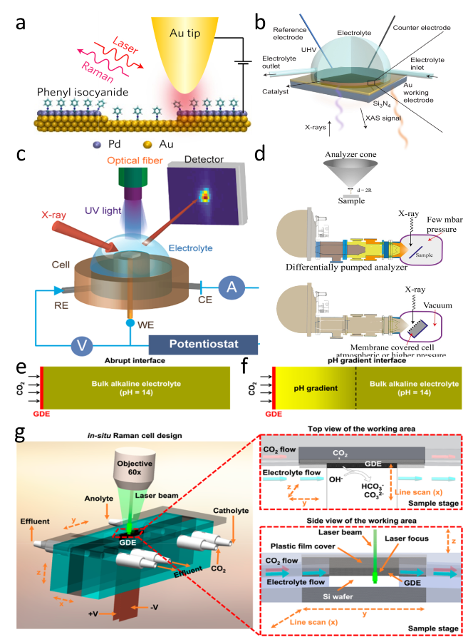
Figure 9. (a) Schematic of an STM-based time-dependent tip-enhanced Raman spectroscopy (TERS).[140] Copyright 2016, Nature Publishing Group. (b) Schematic illustration of the in situ XAS liquid cell.[142] Copyright 2018, Nature Publishing Group. (c) Schematic of the experimental setup for operando X-ray reflectivity of SrTiO3.[141] Copyright 2016, American Chemical Society. (d) Schematic illustration of the in situ XPS experimental set-up.[143] Copyright 2018, Wiley-VCH Verlag GmbH & Co. Designed flow cell for performing in situ Raman measurements to distinguish between (e) an abrupt interface and (f) a gradient interface. (g) The cell design with both top and side views of the cathode area.[144] Copyright 2020, American Chemical Society. |
Table 1 Summary of on-chip HER electrocatalytic devices. |
| Strategies | Types | Materials | Performances | Electrolyte | Ref. |
|---|---|---|---|---|---|
| Identification of active sites | Basal and edge | 2H and 1T'-MoS2 monolayers | (2H)basalη10=−425±27 mV Edge η10=−201±42 mV (1T')basalη10=−356±41 mV Edge η10= −77 ± 24 mV | 0.5 M H2SO4 | [64] |
| 2H-MoS2 basal plane with the vacancy | η10 ≤ −150 mV | 0.5 M H2SO4 | [80] | ||
| helical WS2 | η=−560 mV (vs Ag/AgCl) (20 nA μm−2) | 0.5 M H2SO4 | [104] | ||
| WTe2 | η(100)= −320 mV | 0.5 M H2SO4 | [105] | ||
| phase and layer | 1T'-MoS2 2H/1T′-MoS2 | η= −65 mV η= 200 mV | 0.5 M H2SO4 | [82] | |
| Heterophase boundaries between the 2H and 1T’ phases in MoTe2 | η= -210 mV | 0.5 M H2SO4 | [107] | ||
| PtSe2 | Monolayer η=60 mV Thick η=550 mV | 0.5 M H2SO4 | [106] | ||
| Catalytic window | 2H-MoS2 | η=−290 mV | 0.5 M H2SO4 | [108] | |
| Monitoring the performance at a single material. | GBs and S vacancies | MoS2 nanograin film | η10=−25 mV | 0.5 M H2SO4 | [112] |
| Doping | P-MoS2 | η10=−297 mV | 0.5 M H2SO4 | [113] | |
| V-MoS2 | η10=−185 mV | 0.5 M H2SO4 | [116] | ||
| Design single atom | Mo-MoS2 | η10=−107 mV | 0.5 M H2SO4 | [145] | |
| Amorphous PtSex | η=−100 mV | 0.5 M H2SO4 | [115] | ||
| Construct Heterostructure | MoS2/graphene | η10=−110 mV | 0.5 M H2SO4 | [105] | |
| Methylene blue (MB)/MoS2 interfaces | η10=−206 mV | 0.5 mM MB | [118] | ||
| Electric Field Modulation | MoOx/MoS2 core-shell nanowires | η=−200 mV | 0.5 M H2SO4 | [119] | |
| MoS2 at the gate voltage of 5 V | η10=−38 mV | 0.5 M H2SO4 | [120] | ||
| VSe2 | η10=−126 mV | 0.5 M H2SO4 | [81] | ||
| WSe2 with back-gate voltage 20 V | η10=−280 mV | 0.5 M H2SO4 | [124] | ||
| (CoPc)/MoS2 with back-gate voltage 2V | η10=−238 mV | 0.5 M H2SO4 | [130] | ||
| Pt SAs on n-type MoS2 with Vg +40 V | η10=−20 mV | 0.5 M H2SO4 | [130] | ||
| Thermal Modulation | inert MoS2 ML basal plane at 60 °C | η10=−90mV | 0.5 M H2SO4 | [131] |
3.3 Oxygen evolution reaction (OER) on-chip device
The OER is an integral aspect of the water-splitting process, which is considered an environmentally friendly method for producing hydrogen.27, 146-148 The effectiveness of catalysts in the OER is highly dependent on their ability to facilitate charge transfer. Therefore, analyzing the evolution of these conductivity properties during the OER is essential for understanding their catalytic performance.[149-151] For instance, Mai and colleagues utilized on-chip temporal I-V measurements to reveal that oxygen present in the electrolyte inhibited the OER process. This presence led to high initial resistance and a decreased hydroxyl ion density at the catalyst interface, resulting in poor kinetics and reduced catalytic performance.[152]
Nickel-based oxides and hydroxides are widely recognized as effective catalysts for the OER in alkaline conditions. In this regard, Ding et al. have reported enhanced OER activity of γ-NiOOH through the strategic doping of various metals, including Mo, W, Fe, Ru, Co, Rh, and Ir.[153] The ETS measurements of the doped γ-NiOOH demonstrated a significant correlation with the observed improvements in OER activity. This increase in intermediate conductivity can be attributed to the intrinsic connections associated with double exchange (DE) interactions exhibiting differing d-orbital occupancies. These findings put forth a robust methodology for monitoring changes in the electrocatalytic process and contribute to the mechanistic evaluation of the system.
Recently, phosphorus-doped transition metal oxides and transition metal phosphides (TMPs) have verified high performance for the OER, showing the potential to replace common commercial catalysis like IrO2 and RuO2.[154-158] The high performance of TMPs and phosphorus-doped oxides is largely attributed to the process of surface reconstruction that occurs during the OER. Consequently, it is crucial to investigate the specific mechanisms of the intermediates and their functional roles. In their research, Mai et al. implemented targeted measurements to examine the continuous evolution of electric conductance in the reconstructed lattice of P-Co3O4.(Figure 10c).[159] Their findings indicate a significant correlation between electrocatalytic activity and the conductivity of P-Co3O4 during the reconstruction phase. Furthermore, utilizing a specialized microdevice, real-time resistance measurements revealed that the reconstructed P-Co3O4 exhibits superior conductivity compared to the original material. This distinction is evident compare the initial stages of the OER, where both samples initially demonstrate similar electric conductance. Supporting experimental data and DFT calculations have highlighted the coupling effect of P-O groups during the catalytic process. The inclusion of P-O groups modifies the covalency between Co 3d and O 2p orbitals, effectively lowering the free energy barrier and thereby enhancing OER activity. These findings provide insight into a challenge that traditional electrocatalytic measurements often struggle to address: understanding the true function and mechanisms of TMPs or phosphorus-doped oxides during the reconstruction that occurs throughout the OER process. This unique on-chip microdevice platform provides in situ multi-dimensional electrochemical information for complex OER kinetic, enabling a deeper understanding of catalytic reaction mechanisms and offering applications in related fields to investigate dynamic behaviors at the nanoscale.
3.4 Water splitting on-chip device
Electrochemical water splitting is a critical process that encompasses both the HER and the OER, which occur simultaneously at the cathode and anode within an integrated circuit.[160-162] To effectively initiate these reactions, voltages exceeding the theoretical threshold of 1.23 V are generally required to achieve water cracking. Bifunctional catalysts play a crucial role in facilitating both the anode and cathode reactions during the water splitting process. By enhancing the efficiency of these reactions, they contribute to a more streamlined preparation process and help to lower associated costs. Their significance has established them as a primary topic of overall water decomposition for practical applications.[163-165] Chen et al. utilized a synergistic atomic method to facilitate the lateral growth of Cr-doped WSe2 on graphene in a stitching manner.(Figure 10a, b)[85] The bipolar characteristics of the Cr-doped WSe2/graphene system present promising opportunities for the development of innovative bifunctional microreactors aimed at neutral water splitting. Analysis via EIS demonstrated that Cr doping significantly enhances charge transfer for both anode and cathode reactions. Furthermore, the self-stitching capability of graphene effectively reduces the contact resistance within these micro-devices, thereby lowering the energy barrier associated with water splitting. This research not only introduces a novel stitching contact method for synthesizing bifunctional Cr-doped WSe2/graphene heterojunctions but also broadens the application of micro-devices by designing advanced reactors for water splitting.
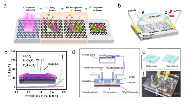
Figure 10. (a) Schematic of the formation process of the Cr-WSe2/graphene heterojunction. (b) Schematic of the on-chip electrocatalytic device.[85] Copyright 2022, American Chemical Society. (c) In situ I-V measurements of individual Co3O4, P0-Co3O4 and P-Co3O4 thin-films. Inset: The schematic of in situ I-V measurements. The applied potentials in WE1 and WE2 (called V1 and V2) increase synchronously vs. RHE, from 1 to 1.8 V, and keep the constant tiny potential difference ΔV (ΔV=1 mV).[159] Copyright 2021, Elsevier Ltd. All rights reserved. (d) On-chip electrochemical measurement setup for the ORR. (e) Schematic illustration of the setup. (f) Schematic diagram of the static and microfluidic PDMS cells.[84] Copyright 2022, Wiley-VCH Verlag GmbH & Co. |
3.5 Oxygen reduction reaction (ORR) micro-device
In addition to the HER and the OER, on-chip nanodevices integrated with ETS represent a highly effective in situ analysis technique. This methodology provides critical insights into electrochemical surface states across a variety of complex reactions, including the ORR.[166-169] For example, research conducted by Duan and colleagues examined the relationship between the kinetics of the ORR and the surface adsorption of various anions on platinum catalysts.[170] Their findings reveal that ETS facilitates the direct visualization of distinct adsorption characteristics and quantitatively demonstrates that competitive anion adsorption can inhibit the adsorption of reactants or the formation of intermediates. This interaction leads to catalyst poisoning and ultimately hampers ORR kinetics. While these studies have illuminated important mechanisms underlying two-dimensional electrocatalysts, most work has focused on static electrocatalytic processes with relatively simple products. To address this limitation, He and his team have successfully developed an on-chip electrocatalytic microdevice that incorporates a sealed electrochemical reservoir. This device is specifically engineered to facilitate the study of diffusion-controlled ORR at the microscopic scale, as illustrated in Figure 10d-f. This significant advancement enhances the methodologies utilized for investigating diffusion-controlled electrocatalytic reactions and guide us in exploring additional details regarding the catalytic reaction.[84]
Nafion is a widely utilized polymer recognized for its role as a stabilizer in catalysis due to its exceptional proton conductivity. However, it can adversely affect the ORR by occupying active sites on the catalyst, which may hinder catalytic performance. Current research predominantly concentrates on Nafion itself, often employing in-situ measurements, with limited investigation into its impact for surface intermediates. In light of this, Sun et al. employed ETS to examine the influence of Nafion on intermediates in the ORR process. The results of the study indicate that Nafion enhances the adsorption of oxygen intermediates with lower binding strength, which significantly impacts reaction selectivity. They found that the kinetics of the platinum-catalyzed ORR transition from a four-electron pathway to a two-electron pathway.[171] Additionally, the integration of PtCu nanoparticles has been shown to mitigate the adsorption of Nafion, thus preserving reaction selectivity. The strategy of ETS for dynamic monitoring offers valuable insights into the ORR mechanism and enhances our understanding of the catalytic process.
3.6 CO2 reduction reaction (CO2RR) and Nitrogen reduction reaction (NRR) on-chip device
The in-situ technique is applicable to a range of electrochemical reactions beyond the HER, such as the CO2RR and the NRR. CO2 is a significant component of the atmosphere and one of the primary contributors to the greenhouse effect. It presents opportunities for transforming high-value products through efficient economic processes, which can help address environmental challenges and advance the goal of carbon neutrality. A comprehensive understanding of the mechanisms underlying CO2RR is essential for advancing our knowledge of various electrochemical processes. Ding et al. introduced a sophisticated technology and testing protocol to quantitatively assess hydrogen sorption on the surface of Pd. Their research primarily focuses on the intermediate products associated with hydrogen and the subsurface palladium hydride (PdHx). They employ in situ conductance measurements facilitated by a microdevice to conduct their analysis. (Figure 11a-e).[172] By combining ETS with on-chip cyclic voltammetry (CV), they clarified the competitive dynamics between CO2RR and hydrogen sorption, emphasizing the critical role of electrolytes—specifically, proton donors with varying pKa—in determining hydrogen sorption kinetics and CO2RR performance. Moreover, they showed that a weakened metal-hydrogen (M-H) interaction in alloy catalysts could enhance CO2RR performance, influenced by the local electrolyte environment. The research conducted by the Ding group involved the employment of real time on-chip techniques to investigate the operando states of monolayer Bi2WO6 during the CO2RR process. Their findings confirmed and proposed the presence of a metallic intermediate in the CO2 reduction process utilizing Bi2WO6, which offers significant insights into the conversion of CO2 into formic acid.[174]
Nitrogen, constituting approximately 80% of Earth's atmosphere, exists in the highly stable gaseous form (N2) under normal conditions. Transformation of N2 into ammonium salts, primarily achieved by nitrogenase in bacteria, presents a significant challenge. Consequently, developing artificial catalysts with inorganic structures that mimic these natural processes could enhance our understanding of nitrogen fixation catalysis. Using on-chip microcells, Zhang et al. investigated NRR performance of Co-doped MoS2-x with sulfur vacancies.[175] They selectively exposed the basal plane of both MoS2-x and Co-doped MoS2-x. demonstrating improved performance in the latter through polarization curve analysis. This microcell platform facilitated an investigation into the synergistic effects of Co doping and vacancies, paving the way for more efficient electrochemical NRR catalyst design.
3.7 Bio-electrochemical on-chip device
The micro-device presented demonstrates significant potential for application in bio-electrocatalytic contexts. Extracellular electron transport (EET) is defined as the transfer of electrons from cells to outside the cell, a process that is vital for global biogeochemical cycles[176] and is known as a foundational principle underlying microbial fuel cell technologies and the production of microbial biofuels.[177] Historically, there have been discussions regarding two primary models that explain the mechanisms of EET, focusing on the structural characteristics of microbial cells and their extracellular matrices. The first model posits that electron conduction is primarily driven by redox activity, which relies on the hopping of electrons between adjacent cofactors. In contrast, the second model suggests that the conductivity of Geobacter biofilms is facilitated by delocalized electronic states within microbial through π−π stacking interactions of aligned aromatic moieties in the pili.[178] Understanding the precise mechanisms involved is essential for a comprehensive grasp of the functional and structural aspects of these electrogenic microbial systems. In a notable study, Ding et al. conducted systematic on-chip electrical transport investigations on Shewanella oneidensis MR-1 and Geobacter sulfurreducens PCA under physiological enviroment.(Figure 11g1-g6).[173] Their findings indicate that the electrical conductivity observed in MR-1 is due to the charge transfer occurring at the cell/electrode interface. Additionally, they identified the electrode area as a critical factor influencing charge transfer, thus supporting the first model that relates electron conduction primarily to redox reactions. thereby rendering the achievement of metallic-like conduction challenging. This research provides substantial evidence regarding the electrical transport mechanisms in microbial cells and enhances our understanding of microbial communities engaged in bio-electrocatalysis.
The recent advancements in machine learning (ML) technology have facilitated the development of models that improve performance through the training of both experimental and theoretical data. This progress presents promising in silico design principles and high-throughput screening methodologies, which are crucial for the future development of volatile organic compound (VOC) sensory arrays across a variety of application scenarios. In their research, Ding et al. successfully fabricated two-dimensional materials that integrate a range of single atomic sites for the monitor of VOCs at normal temperature.[179] The incorporation of these SASs serves as an important role in enhancing the sensitivity, selectivity, and response/recovery time of the sensing devices. By employing a series of structurally similar yet chemically distinct SASs, they were able to construct sensitive sensory arrays that demonstrate heightened selectivity for different analytes.
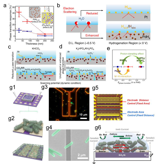
Figure 11. (a) The relationship between the thicknesses of Pd and Pd4Ag nanowire films and their phase transition responses (ΔRMHx) is illustrated on the ETS. (b) Schematic of electron scattering in metals with surface adsorbates and hydrides. A schematic of the different Pd-H states in (c) KHCO3 and (d) K2HPO4/KH2PO4 and the corresponding CO2RR processes at the interfaces. (e) Summary of phase transition potentials of Pd and Pd4Ag under CO2RR conditions in KHCO3 and K2HPO4/KH2PO4 obtained at 10 mV/s.[172] (g1, g2) Schematic of the nanoelectronic measurement setup. (g3) Optical microscope (OM) image of MR-1 in dark-field mode. (g4) An ex situ SEM image of MR-1. (g5) Schematic of biofilm measurements. (g6) Schematic of the electrochemistry model at the interface of Shewanella oneidensis MR-1.[173] Copyright 2016, American Chemical Society. |
3.8 Photoelectrochemical on-chip device
Solar cells, recognized as clean and renewable energy sources, have gained considerable attention for their potential application for nanoelectronic field, particularly in light of advancements in miniaturization. The current investigation into microscopic materials presents a significant opportunity for the development of miniature products, while also enhancing the efficiency of photovoltaic systems.[182-189] For instance, Yang et al. has developed p-i-n coaxial Si nanowire photoelectrochemical device, which has achieved high energy conversion efficiency.(Figure 12a-d).[91] Si nanowires are utilized in photovoltaic applications, serving as an innovative power source that enhances the potential applications of nanoelectronics, facilitating innovative research into photoinduced energy and charge transport, as well as artificial photosynthesis.[190] In addition to nanowires, two-dimensional (2D) materials are critical in photoelectrochemistry, due to their unique atomic planer with potential active sites and efficient charge transfer. The investigation of photoelectrochemical application of these layered materials at the single-layer level presents significant challenges when using conventional measurement techniques. A noteworthy study conducted by Kostya S. Novoselov and his colleagues focused on MoS2 with varying layer counts.[191] They employed a microcell setup to systematically examine the catalytic performance of localized MoS2 films under various irradiation conditions. By utilizing redox mediator, specifically [Ru(NH3)6]3+/2+, to assess charge transfer information, along with LiCl for electric double-layer capacitance (EDLC), their research reveals a substantial dependence of catalytic performance on both the thickness of MoS2 and the intensity of illumination. Such on-chip microcells not only enhance the measurement capabilities for the electrochemical behavior of individual nanosheets but also lend themselves to seamless integration with solar simulators.
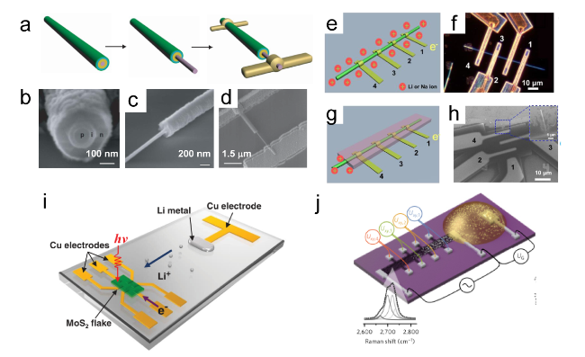
Figure 12. (a) Schematics of fabrication process of the single nanowire photovoltaic device. (b, c, d) SEM images corresponding to schematics in a.[91] Copyright 2007, Nature Publishing Group. (e, f) The schematics and dark field optical microscopic image of the nanowire electrode. (g) The second configuration, in which the nanowire is covered by a passivation layer with only one exposed end. (h) The SEM image of the device with the second configuration.[79] Copyright 2015, American Chemical Society. (i) Schematic of MoS2-Li microbattery.[180] Copyright 2015, Wiley-VCH Verlag GmbH & Co. (j) Schematic of the device for lithium ion diffusion in bilayer graphene. The inset shows the Raman scattering response of bilayer graphene.[181] Copyright 2017, Nature Publishing Group. |
3.9 Mechanism analysis
On-chip micro-device provided multi-dimensional insights for the small and precise perspective. DFT elucidates the fundamental properties and reaction dynamics that offer valuable insights into the mechanisms underpinning electrocatalytic processes. Many research works have been reported that relying the micro cell, theoretical calculation can calculated the density of states (DOS), Gibbs free energy of adsorption ∆GH*, adsorption/dissociation energy, reaction kinetics path and so on for more refined structure. Therefore, with the development and integrated of such analysis technology, it can provided more comprehensive and detailed for catalytic mechanism and guide to design high performance catalyst. Liu et al. utilized vanadium (V) doping to investigate the synergetic effect of vacancies and heteroatom doping in the catalyst.[116] On-chip electrochemical tests provided valuable experimental information, with typical configuration to study the synergetic effect of vacancies and V doping. As shown in Figures 13a-b, SubV is primarily divided into three cases: ordinary doping with no vacancy (Ord.), one vacancy atom connected to a S vacancy (VacS), and one vacancy atom connected to an adjacent Mo atom (VacS(Mo)). Sub2V consists of three arrangements: two vacancy atoms organized in meta-position (Meta), mal-position (Mal), or adjacent position (Adj.). Sub3V includes vacancy-free arrangements (Meta and Mal) as well as complex arrangements (Adj.-1 and Adj.-2). Based on the model, different H adsorption sites for different configurations, along with the ∆GH* for all defect configurations, are calculated to demonstrate the optimization of MoS2 catalytic performance.
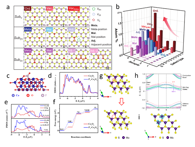
Figure 13. (a) Illustration of atomic defects observed in single-layer V-MoS2. (b) Statistical analysis of the concentration of these atomic defects.[116] Copyright 2022, Wiley-VCH Verlag GmbH & Co. (c) Structural diagram of P-Co3O4. (d) Total electronic density of states for Co3O4 and P-Co3O4. (e) Calculated PDOS of Co3O4 and P-Co3O4. (f) Calculated free energy diagram of the OER on Co3O4 and P- Co3O4.[159] Copyright 2021, Elsevier Ltd. All rights reserved. (g) The schematic of the S vacancy site created on the modeled MoS2 surface. (h) The computed band structures of the MoS2 surface with 5.5% S vacancies at various induced charge levels. (i) The charge density difference of a monolayer of MoS2 with 5.5% S vacancies.[192] Copyright 2019, American Chemical Society. |
Integrating on-chip EIS data, which provides detailed micro-level insights, with theoretical simulations enhances the analysis from an atomic perspective and enables a thorough investigation of potential mechanisms. In their study, Mai et al. employed this methodology to investigate the impressive OER performance of reconstructed lattice P-doped oxides. Their findings reveal an induced electronic coupling between the newly formed oxides and P-O groups.[159] Figures 13c-f present the total electronic density of states (TDOS) for both P-Co3O4 and Co3O4. The electron-occupied states near the Fermi level for P-Co3O4 closely resemble those of Co3O4, which results in comparable intrinsic conductivity. Additionally, the projected density of states (PDOS) analysis indicates the coupled P-O groups modify the positions of the metal and oxygen band center, reducing the energy discrepancy (from 1.51 eV to 1.15 eV). Consequently, P-Co3O4 demonstrates enhanced metal and oxygen orbital hybridization and covalency strength compared to Co3O4. The enhanced covalency of the Co-O bond promotes efficient charge transfer between the metallic center and the oxygen adsorbates, thereby improving the overall activity for the OER.
Frisbie et al. utilized DFT to examine the charge states at active sites under back gating conditions. Their research demonstrated that the superior performance in the HER can be attributed to the enhanced strength of the Mo−H bonds. The enhanced strength observed is attributed to the electronic charge present on the Mo metal, which results from the implementation of back gating.[192] ( Fig. 13g-i)
4 Energy storage devices
4.1 Battery on-chip device
As societal energy demands continue to rise, the advancement of next-generation energy storage become progressively more important.[193, 194] Efficiency is a critical factor in energy conversion, underscoring the need for more effective, compact devices that meet today's energy requirements.[195-197] Micro- and nanomaterials have shown great promise in enhancing energy conversion efficiency. On-chip devices serve as multi-functional platform for real-time measurement, helping to elucidate mechanisms related to energy storage and capacity fading, which are essential for developing high-performance electrode materials. Mai group developed an all-solid-state device utilizing a single nanowire, which establishes a direct link between electrical transport and structural changes during charging and discharging cycles. Their findings indicated that capacity decay and conductivity loss were linked to structural damage in the nanowires.[72] They also observed that while the structural changes during shallow charge and discharge were reversible, more intense cycling resulted in irreversible damage to the silicon nanowires.
Lithium-ion batteries represent one of the most promising advancements in rechargeable energy sources. Their application is widespread, particularly in portable electronics and electric vehicles, highlighting their significance in today’s technology landscape.[198-200] However, due to the limited abundance of lithium and its high cost, researchers are increasingly exploring sodium-ion batteries, particularly for stationary grid storage, as they offer lower production costs. Despite this, most studies focus on battery performance metrics, the mechanisms of Li+ and Na+ transport in micro-device have not been extensively investigated. In response to this gap, Xu et al. developed single nanowire devices with multiple contacts to investigate the ion transport mechanisms in these nanoscale electrode materials. Their work contributes valuable insights into the behavior of lithium and sodium ions, advancing our understanding of nanoscale electrode performance. (Figure 12e-h).[180] By employing different configurations—one fully immersed in electrolyte and another with one end exposed—they found that conductivity decreased after ion intercalation for both lithium and sodium, indicating similar electrochemical reaction mechanisms. However, sodium ions caused more significant conductivity degradation and structural damage due to their larger volume and greater energy barriers. [200]
On-chip microcells provide a platform for detailed in situ measurements that reveal optimization mechanisms in energy storage systems. For example, Hu et al. assembled nanowire devices made from pure MnO2 and composites with reduced graphene oxide (rGO) and porous graphene (pGO) to explore the effects of graphene on energy storage.[200] Their electrochemical measurements showed that while rGO significantly enhanced the conductivity of MnO2, it also reduced ion diffusion rates—a challenge effectively addressed by using pGO, which allowed for ion transport through both the gaps and pores. Liao et al. utilized on-chip microcells to investigate the role of heterostructures in electrochemical reactions, revealing differing capacities and ionic diffusion properties in MoS2 and MnO2.[201] Their in situ I-V measurements indicated that these differences were influenced by unilateral conduction, providing valuable insights for designing heterostructured electrode materials. Layered materials, particularly those with significant van der Waals gaps, such as MoS2 and graphene, are well-suited to serve as hosts for ion transport.[202, 203] Cui’s group also explored MoS2 by electrochemically inserting lithium ions into its interlayer spacing, observing significant enhancements in light transmission and electrical conductivity due to changes in band structure. They documented the intercalation process visually, showing a pathway from the edge to the center of the MoS2 nanosheet. Additionally, Hu’s group designed a planar microbattery that enables in situ electrical transport measurements during electrochemical charge and discharge in micron-sized MoS2 crystallites, alongside optical studies that inform about the electronic structure. (Figure 12i)[180] They found that the electrical conductivity of 2D MoS2 crystallites was highly dependent on thickness and lithiation rates.
Kühne group utilized micro-device to study Li+ diffusion in bilayer graphene, emphasizing that efficient charge transfer is a crucial indicator of the lithiation state in electrode materials. (Figure 12j)[181] Their observations of densely packed lithium atoms in bilayer graphene suggest a multi-layered close-packed structure.[204] The investigations offer a distinct methodology for examining the structural evolution that occurs during charge and discharge cycles through in-situ measurements. The integration of in-situ conductance measurements, along with quantitative data and in-situ spectroscopy, greatly facilitate the advancement of on-chip energy field devices.
4.2 Micro-supercapacitors on-chip device
As miniaturized electronic devices advance, there is increasing demand for affordable micro energy storage solutions.[208-210] Microcapacitors are essential components in integrated circuits, and as circuit integration technology evolves, so too does the manufacturing process for functional capacitors, particularly metal-plate capacitors.[211, 212] This evolution is crucial for micro-supercapacitors, which require stringent criteria for electrode materials and device fabrication to optimize key performance characteristics.
Pan et al. developed a novel protocol that mimics the spider's silk-spinning process to fabricate highly oriented microfibers from graphene-based composites using a specially designed microfluidic chip. The microfibers are strategically arranged in a planar configuration to develop asymmetric micro-supercapacitors designed for flexible and on-chip energy storage applications.[213] Mai's research team employed a sophisticated approach to achieve remarkable power and energy densities in microsupercapacitors. This was accomplished through the strategic integration of pillar arrays within microspirals. (Figure 14b-d)[206] This innovative approach enhances the efficiency of electrical transport, facilitating improved accessibility for ions (cations and anions) within the electrolyte to reach the surface of the nanosheets. Additionally, it effectively minimizes the risk of detachment of active materials during the fabrication process. Additionally, the unique micro-scale spiral design enables the creation of shape-engineerable micropseudocapacitors and unconventional series/parallel configurations, applicable to various pseudocapacitive materials.
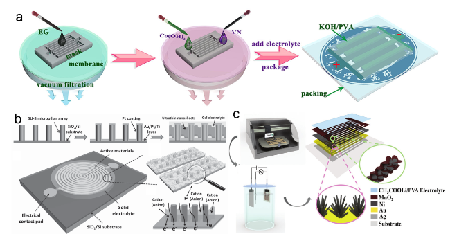
Figure 14. (a) Fabrication and structural characterization of SST-MPCs.[205] Copyright 2018, Nature Publishing Group. (b) Schematic of the fabrication process of SST-MPCs.[206] Copyright 2015, Wiley-VCH Verlag GmbH & Co. (c) Schematic of the printable fabrication procedure.[207] Copyright 2017, Wiley-VCH Verlag GmbH & Co. |
Lin et al. demonstrated the potential of inkjet-printing technology to produce artistically designed electrode patterns for working supercapacitors. This method not only achieves aesthetically pleasing designs but also illustrates high scalability, as evidenced by the production of larger artistic supercapacitors that function within a wearable self-powered system. (Figure 14e)[207] Xiao group introduced a facile, mask-assisted fabrication method for micro-supercapacitors, utilizing interdigital hybrid electrodes composed of stacked phosphorene nanosheets and electrochemically exfoliated graphene in ionic liquid electrolytes. This technique allowed for the direct manufacturing of hybrid films with exceptional uniformity, flexibility, and conductivity, serving as binder- and additive-free flexible electrodes for micro-supercapacitors. This marks the first application of phosphorene in micro-supercapacitor fabrication, achieving high energy densities. Moreover, they assembled 2D VN nanosheets and Co(OH)2 nanoflowers to create asymmetric devices with high volumetric energy density.(Figure 14a)[205] Additionally, lithium-ion capacitance materials, such as carbon-coated Li₄Ti₅O₁2, have been reported for use in hybrid micro-supercapacitors.[214] The study by Mai’s group on 0D, 1D and 2D carbon materials emphasizes the critical interplay between the selection of electrode materials, the construction of current collectors, and the overall constitution of devices.[215, 216] This interplay remains a critical area for evaluation, particularly in the context of new microfabrication processes.
5. Conclusion and perspective
This review highlights the primary applications of micro-/nanodevices for in-situ characterization of electrochemical reactions, with a particular focus on electrocatalysis. Research targeting nano-device-based systems has significantly advanced our understanding of underlying mechanisms. Concurrently, the rapid development of portable and embedded micro-/nanodevices has propelled the progress of micro energy conversion and storage technologies. Initially, an on-chip device was developed to identify catalytic active sites for the HER by selectively exposing specific regions of the catalyst, including edges, basal planes, phases, and layers etc. As technology has advanced and research deepened, a variety of electrocatalytic processes and their corresponding configurations have been realized, encompassing the OER, water splitting, ORR, NRR, and CO2RR. Utilizing a four-electrode system with dual-channel measurements (both electrochemical and electrotransport), researchers have uncovered and addressed significant phenomena, such as hydrogen adsorption/desorption (Hupd) on Pt NWs, the self-gating phenomenon, the effects of alkali metal cations in alkaline environments, and the role of adsorbed hydrogen (Had) as a critical intermediate in the kinetics of HER. In the realm of photoelectrochemical devices, a single p-i-n silicon nanowire has been employed as an on-chip solar cell. Additionally, advancements in battery technology have led to the development of high-performance lithium-sulfur (Li-S) on-chip batteries through innovative electrode designs, as well as micro all-solid-state single nanowire batteries intended for in situ monitoring of charge and discharge processes. Furthermore, as a prominent energy storage solution, microsupercapacitors have been successfully synthesized and implemented.
On-chip devices facilitate targeted investigations of individual nanomaterials or specific regions, yet most studies primarily involve nanowires and sheets, with limited exploration of other nanostructures, such as nanoparticles. Given the micro/nanometer scale of the materials, the resultant current signals are inherently small, rendering the data particularly susceptible to disturbances. Consequently, even minor disruptions can lead to significant deviations in results. Addressing challenges such as reducing the noise in electrical lines while minimizing the window size is crucial. Optimizing device structures, enhancing source-measurement unit (SMU) circuits, and exploring alternative insulating layers (e.g., amorphous SiO2 or Al2O₃) could enable simulations of more complex physical and chemical models. Currently, on-chip platforms are predominantly employed in straightforward reactions, HER and OER. Future research could extend to catalytic processes involving smaller molecules (e.g., CO2, N2, and CH₄) within more complex electrolyte systems. DFT is a widely recognized method that offers valuable predictive insights into catalytic performance and the electronic structure of comprehensive catalytic systems. This computational approach effectively integrates detailed information derived from micro on-chip devices, showcasing significant potential for research in the structure-activity relationship and facilitating advancement at microcosmic perspective. Furthermore, with the ongoing advancements in computational, DFT plays a crucial role in elucidating potential mechanisms and in predicting the development of promising catalysts.[217] Monitoring the electrocatalytic process at small active surface sites, along with the transformation of reaction products, will significantly enhance our understanding of the intricate and fundamental mechanisms involved. This approach will contribute to a more comprehensive analysis of the underlying processes.(Figure 15). The use of advanced spectroscopic techniques—such as infrared spectroscopy, Raman spectroscopy, and high-resolution X-ray methods—will play a crucial role in clarifying the behavior of catalytic molecules. This includes processes such as adsorption, activation, and bond cleavage on individual nanomaterials. Moreover, the synergistic effects of field modulation, electric fields, and photoelectric effects on HER performance merit investigation. On-chip devices provide an ideal platform for exploring the influence of various factors, including light, magnetic fields, and temperature. Employing device simulations alongside multiple physical fields not only simplifies theoretical analysis but also enriches experimental data, supporting theoretical models. The use of new machine learning techniques within multiscale device models offers potential benefits for the advancement of electrochemical technologies. With ongoing developments in artificial intelligence and device miniaturization, the potential for self-energizing integrated devices is virtually limitless, particularly when scaled to millimeter dimensions with micro/nano-watt power consumption. Considering the promising future applications, it is essential for researchers to focus on refining their development processes. In addition energy conversion, on-chip micro devices demonstrate considerable promise in areas such as energy storage, biosensing, and medical field. To effectively address integration and monitoring requirements, modifications to device structures will be necessary. Furthermore, prioritizing the mass manufacturability of fabrication processes should be a key consideration in ongoing research efforts. As microfabrication technologies evolve, they will provide new opportunities to uncover fascinating phenomena and address scientific inquiries. The collaborative efforts of experts across various fields will greatly enhance the advancement of microdevices. This synergy is expected to facilitate the exploration and discovery of electrocatalytic principles that have historically been overlooked.
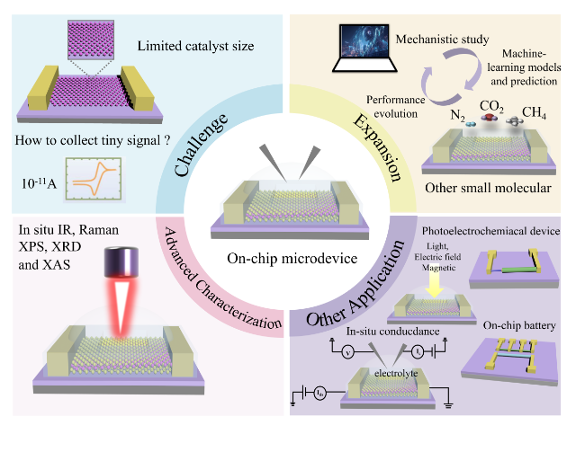
Figure 15. Prospects for on-chip microcells. The challenges in this emergent field, such as limited catalyst size. The applications of the on-chip microcells, e.g., the expansion, other application and advanced characterization are expected. |
Declaration of Competing Interest
The authors declare that they have no known competing financial interests or personal relationships that could have appeared to influence the work reported in this article. Jizhou Jiang is the Editor-in-Chief, Song Liu is an Associate Editor of this journal and they were not involved in the editorial review or the decision to publish this article.