×
模态框(Modal)标题
在这里添加一些文本
Close
Close
Submit
Cancel
Confirm
×
模态框(Modal)标题
×
Editor center
Submit
Search
Toggle navigation
Home
About Journal
Journal Information
Editorial Board
Awards
Journal Metrics
Contact
Journal Online
Just Accepted
Current Issue
Highlights
Archive
Most Read
Most Download
Most Cited
Guide for Authors
Publishing ethics
Publishing ethics
Generative AI policy
Subscribe
Figure/Table detail
Recent advances and applications of on-chip micro-/nanodevices for energy conversion and storage
Haiyan Xiang, Jan E. Lopez, Travis Hu, Jiayuan Cheng, Jizhou Jiang, Huimin Li, Tang Liu, Song Liu
Composite Functional Materials
, 2025, 1(
1
): 20250102. DOI:
10.63823/20250102
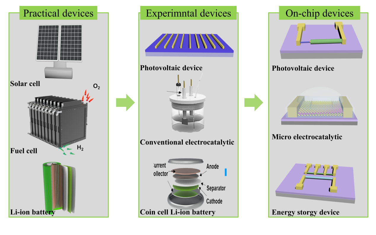
Figure 3.
An analysis of practical configuration, lab testing equipment and on-chip micro-device.
[
96
]
Copyright
2019
, Elsevier Ltd. All rights reserved.
Other figure/table from this article
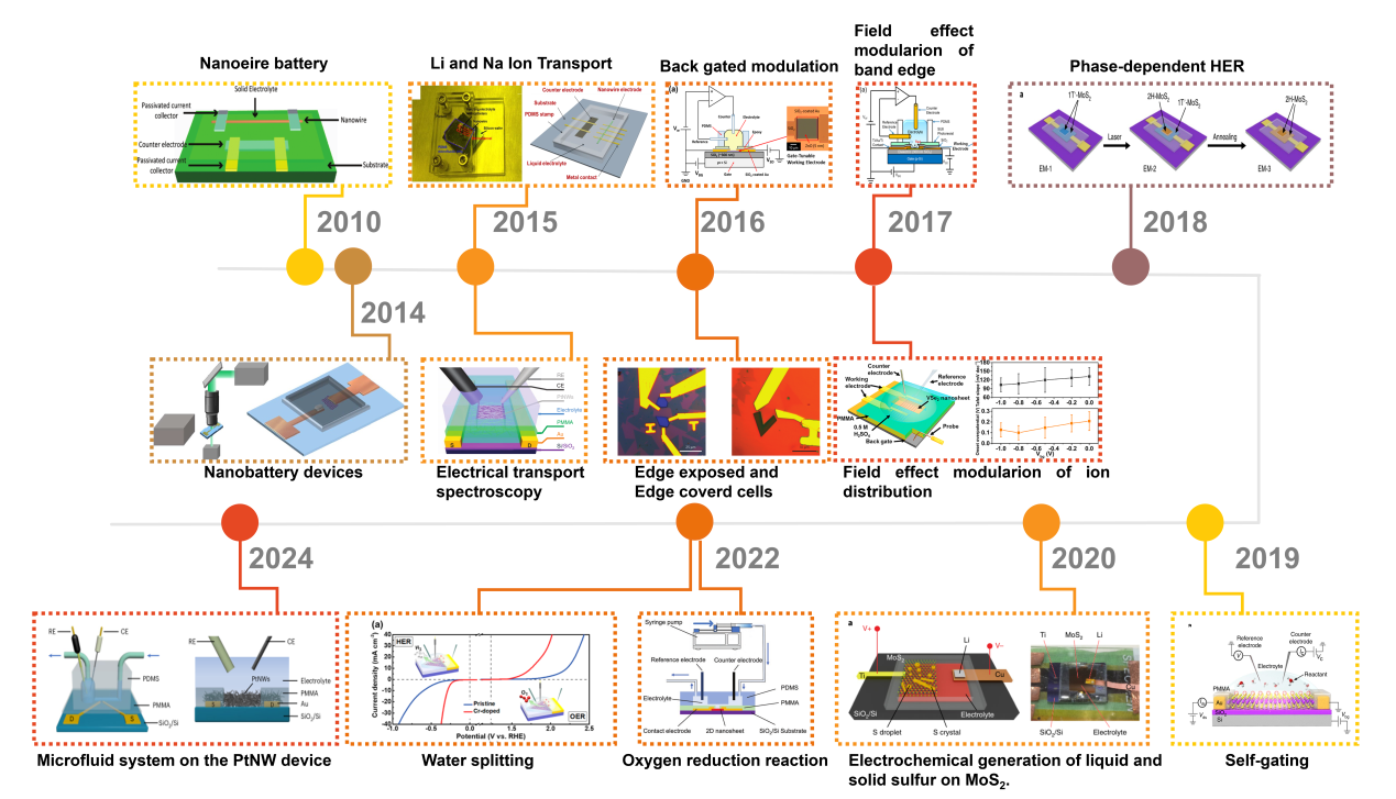
Figure. 1
Timeline for the on-chip microcell in electrocatalysis.
[
77
]
Copyright (
2010
) American Chemical Society;
[
78
]
Copyright (
2014
) Nature Publishing Group;
[
68
,
79
]
Copyright (
2015
) American Chemical Society and Nature Publishing Group;
[
66
,
80
]
Copyright (
2016
) American Chemical Society and Nature Publishing Group;
[
67
,
81
]
Copyright (
2017
) American Chemical Society;
[
82
]
Copyright (
2018
) Nature Publishing Group;
[
69
]
Copyright (
2019
) Nature Publishing Group;
[
83
]
Copyright (
2020
) Nature Publishing Group;
[
84
,
85
]
Copyright (
2022
) Wiley-VCH Verlag GmbH & Co and American Chemical Society;
[
86
]
Copyright (
2024
) Nature Publishing Group.
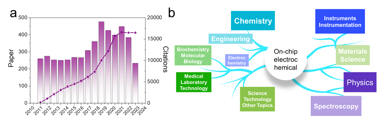
Figure. 2
(a) Annual number of publications by using keyword of “on-chip electrocatalysis” from Web of Science on January 7, 2025. (b) The hot spot in the total circulation.
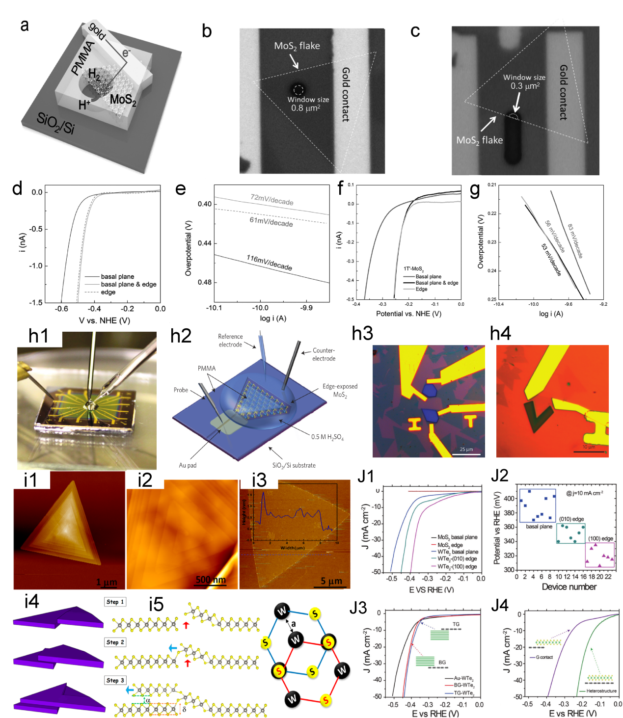
Figure 4.
(a) Schematic of the on-chip setup. Optical image of a MoS
2
showing the (b) basal and (c) edge planes. (d) LSV and (e) Tafel plots of the MoS
2
with basal plane and edge, the electrolyte was argon-purged in 0.5 M H
2
SO
4
and scan rate was set at 10 mV s
−1
. (f) LSV and (g) Tafel curves of monolayer 1T′-MoS
2
basal plane, and edge in HER.
[
64
]
Copyright
2017
, Wiley-VCH Verlag GmbH & Co. (h1) Photograph of the electrochemical microcell. (h2) Schematic of the on-chip electrocatalytic. Optical microscope images of single-layer MoS
2
with (h3) the basal and (h4) edge exposed.
[
80
]
Copyright
2016
, Nature Publishing Group. (i1, i2) AFM of spiral WS
2
domains and (i3) corresponding height of monolayer WS
2
. (i4) Schematic of the spiral domain growth modes. (i5) Schematic of the atomic arrangement in spiral WS
2
.
[
104
]
Copyright
2019
, American Chemical Society. (j1) LSV of MoS
2
and WTe
2
with different exposed area, the overpotential of (100), (010) edge and basal plane is 320 ± 10 mV, 350 ± 10 mV and 390 ± 20 mV respectively at 10 mA cm
−2
. (j2) Summary of the overpotentials for WTe
2
with different exposed sites. (j3) LSV of WTe
2
with basal plane. (j4) LSV of MoS
2
with a graphene contact, as well as from the MoS
2
/graphene heterostructure.
[
105
]
Copyright
2018
, Wiley-VCH Verlag GmbH & Co.
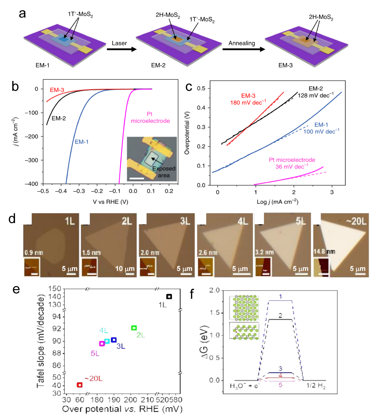
Figure 5.
The diagram of fabrication process. (b) The LSV for EM-1, EM-2, and EM-3, with an inset image EM-1, the overpotential of EM-1 and EM-2 is 165 mV and 200 mV, respectively. Scale bar, 20 μm (c) Tafel plots corresponding the (b).
[
82
]
Copyright
2018
, Nature Publishing Group. (d) Optical images of CVT-grown PtSe
2
flakes ranging from 1 to 20 layers, insets show the corresponding AFM images. (the same height scale for AFM images, the scale bar of first is 1 μm, others is 0.5 μm) (e) LSV and Tafel slops for the HER. (f) ΔG
H
diagram for HER of different layer PtSe
2
.
[
106
]
Copyright
2019
, Wiley-VCH Verlag GmbH & Co.
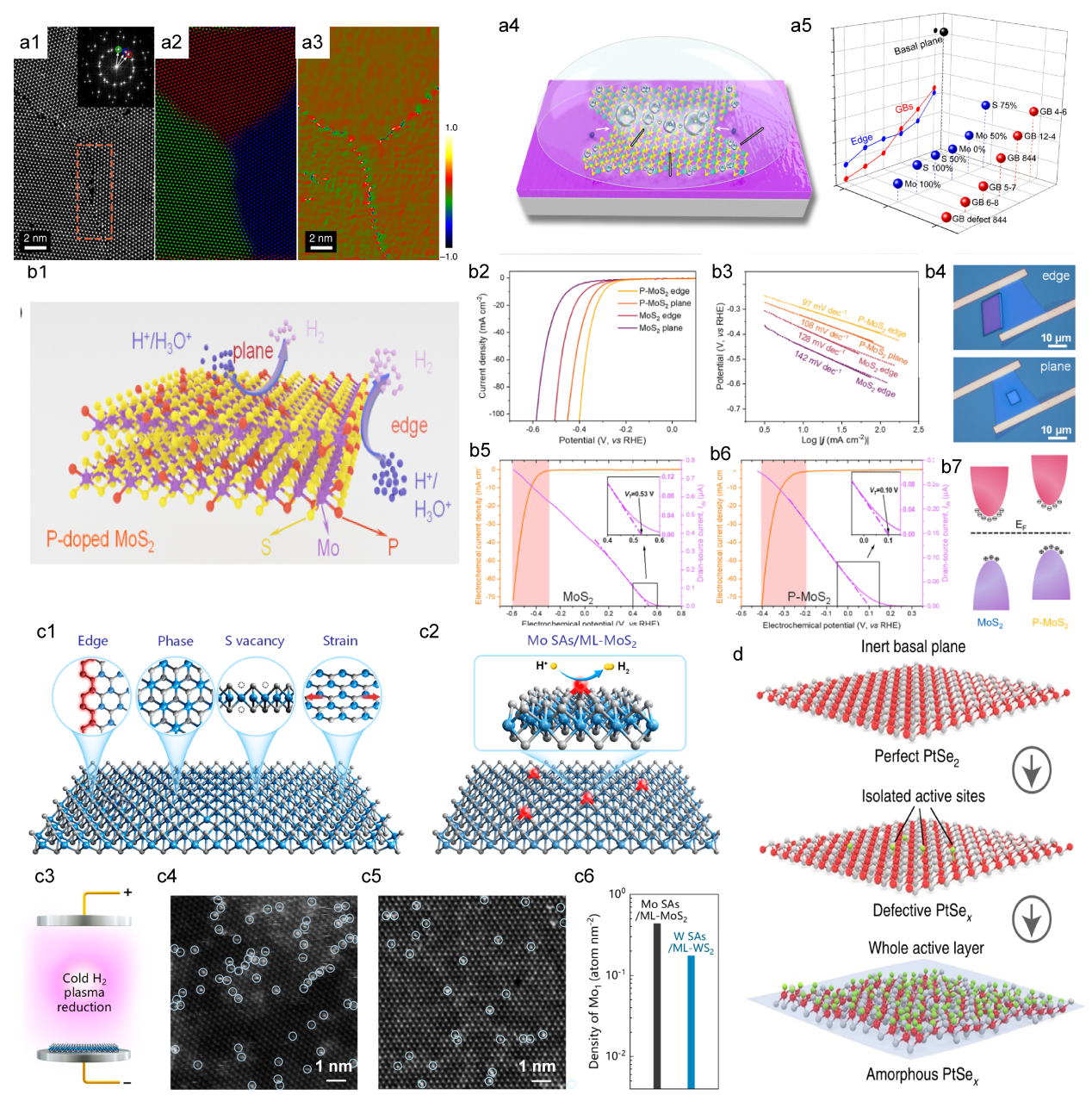
Figure 6.
(a1) The HAADF STEM image of the GBs between three MoS
2
grains, the inset on the left shows the Fourier transform. (a2) The composite color-coded inverse fast Fourier transform (IFFT) image. (a3) illustrates the Geometrical Phase Analysis (GPA) routine.
[
112
]
(b1) Schematic of HER process on P-MoS
2
nanosheets. (b2) and (b3) show the LSV and Tafel plots for the MoS
2
and P-MoS
2
, The edge sites show an onset potential (η
10
) of 297 mV and a Tafel slope of 97 mV dec
−1
for HER, exceeding those of the basal plane with 328 mV and 108 mV dec
−1
. (b4) Optical images of edge and basal plane on a P-MoS
2
. (b5) and (b6) display the electrochemical and electronic signals of a MoS
2
and P-MoS
2
during the HER. (b7) Illustrates the electronic structure of P-MoS
2
, aligning the Fermi levels.
[
113
]
Copyright
2017
, American Chemical Society. (c1) Schematic of the active sites of MoS
2
. (c2) Schematic of Mo ML-MoS
2
. (c3) Details the synthesis of metal SAs on a ML-MoS
2
. HAADF-STEM images in panels (c4) and (c5) depict Mo SAs on ML-MoS
2
and tungsten SAs on monolayer WS
2
samples, respectively. (c6) statistical results on the density of Mo and W SAs on 2D monolayers.
[
114
]
Copyright
2020
, American Chemical Society. (d) Schematic of the amorphous PtSe
x
surface, perfect PtSe
2
and defective PtSe
x
.
[
115
]
Copyright
2022
, Nature Publishing Group.
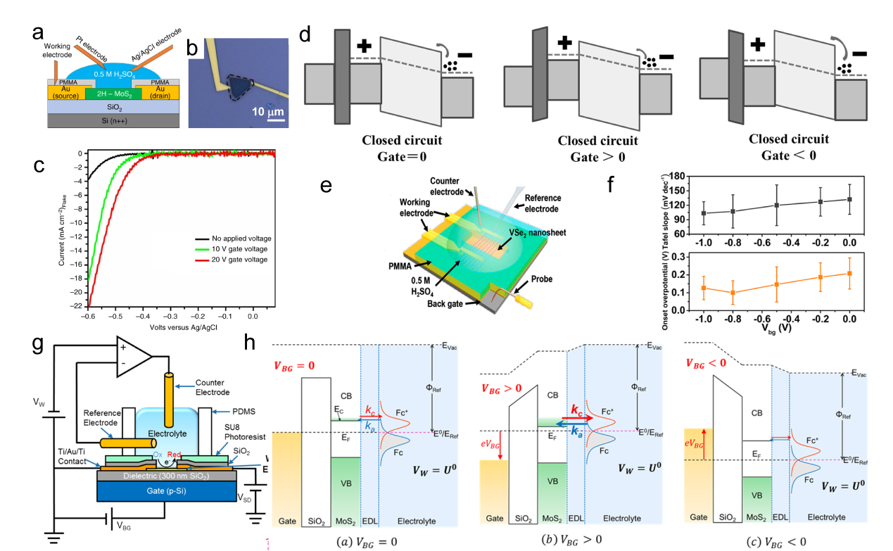
Figure 7.
(a) Schematic of the gate-modulation electrochemical device. (b) Optical images of 2H-MoS
2
with Au pads. (c) LSV of gate-dependent HER measurements, the green and red curves show the improvement in electrocatalytic activity after applying a positive gate voltage of 10 and 20 V, respectively.
[
119
]
(d) Energy band diagrams of the MoS
2
device at different gate bias.
[
120
]
Copyright
2017
, Wiley-VCH Verlag GmbH & Co. (e) Schematic of the HER device under back gate voltages. (f) Statistic-based influence of the back gate on the onset overpotential and Tafel slope.
[
81
]
Copyright
2017
, American Chemical Society. (g) Schematic of a back-gated electrochemical cell. (h) Energy band diagrams of the MoS
2
at various back-gate biases.
[
67
]
Copyright
2017
, American Chemical Society.
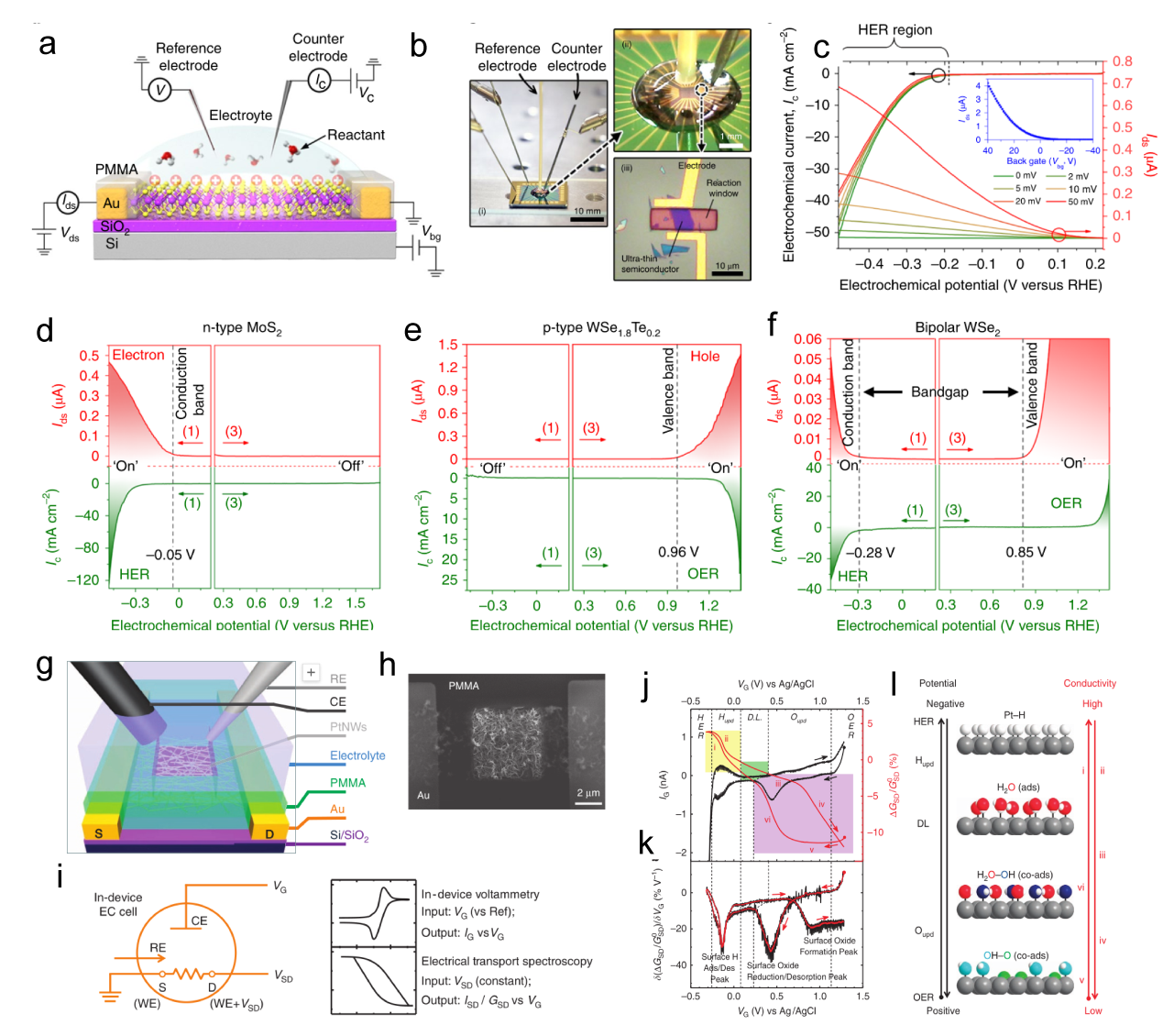
Figure 8.
(a) Schematic of the microcell-based in situ electronic/electrochemical measurement. (b) Optical image of the microcell. (c) Typical electrochemical (y axis in black) and electronic (y axis in red) signals of single-layer WS
2
during the HER at different bias potentials. Self-gating phenomenon of (d) n-type MoS
2
, (e) p-type WSe
1.8
Te
0.2
, and (f) bipolar WSe
2
, typically, n-type MoS
2
is turned on at a negative electrochemical potential and only delivers the HER, p-type WSe
1.8
Te
0.2
is turned on at a positive electrochemical potential and only delivers the OER, bipolar WSe
2
is turned on at both negative and positive electrochemical.
[
69
]
Copyright
2019
, Nature Publishing Group. (g) Schematic of the Pt NW device. (h) SEM image of the device cell. (i) Schematic of CV and ETS for in situ monitoring of the electrochemical interfaces. (j) The I
G
-V
G
and normalized G
SD
-V
G
characteristics of a typical Pt NW device, I
G
-V
G
resembles the typical CV characteristic of a polycrystalline Pt surface, containing redox regions of HER, H adsorption/desorption region (Hupd), double layer (DL) region, surface oxide formation/reduction region (Oupd) and OER. (k) The differentiated ETS curve illustrates spectral peak characteristics. (l) Schematic of various Pt surface conditions along with the sweeping electrochemical potentials (left black axis) and the corresponding changes in conductivity.
[
68
]
Figure 9.
(a) Schematic of an STM-based time-dependent tip-enhanced Raman spectroscopy (TERS).
[
140
]
Copyright
2016
, Nature Publishing Group. (b) Schematic illustration of the in situ XAS liquid cell.
[
142
]
Copyright
2018
, Nature Publishing Group. (c) Schematic of the experimental setup for operando X-ray reflectivity of SrTiO
3
.
[
141
]
Copyright
2016
, American Chemical Society. (d) Schematic illustration of the in situ XPS experimental set-up.
[
143
]
Copyright
2018
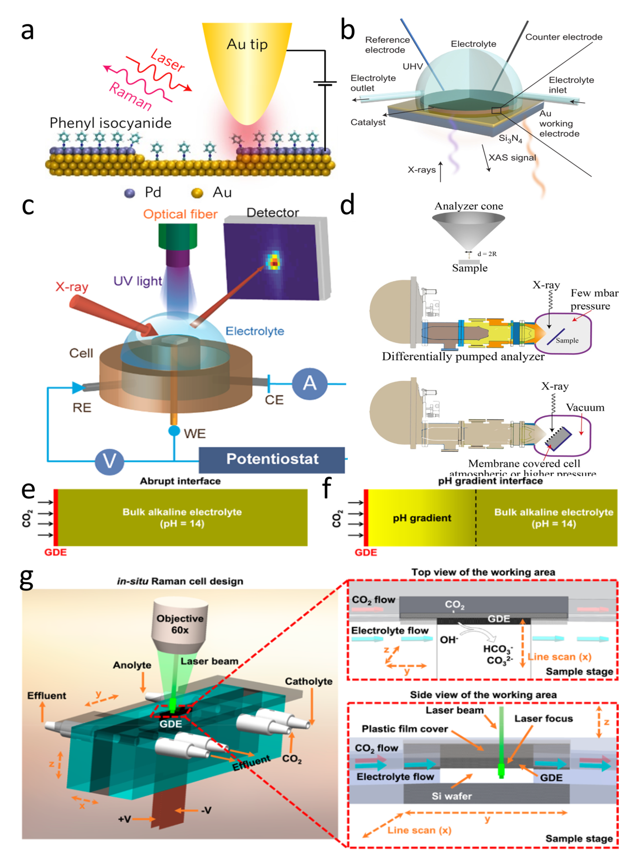
, Wiley-VCH Verlag GmbH & Co. Designed flow cell for performing in situ Raman measurements to distinguish between (e) an abrupt interface and (f) a gradient interface. (g) The cell design with both top and side views of the cathode area.
[
144
]
Copyright
2020
, American Chemical Society.
Table 1
Summary of on-chip HER electrocatalytic devices.
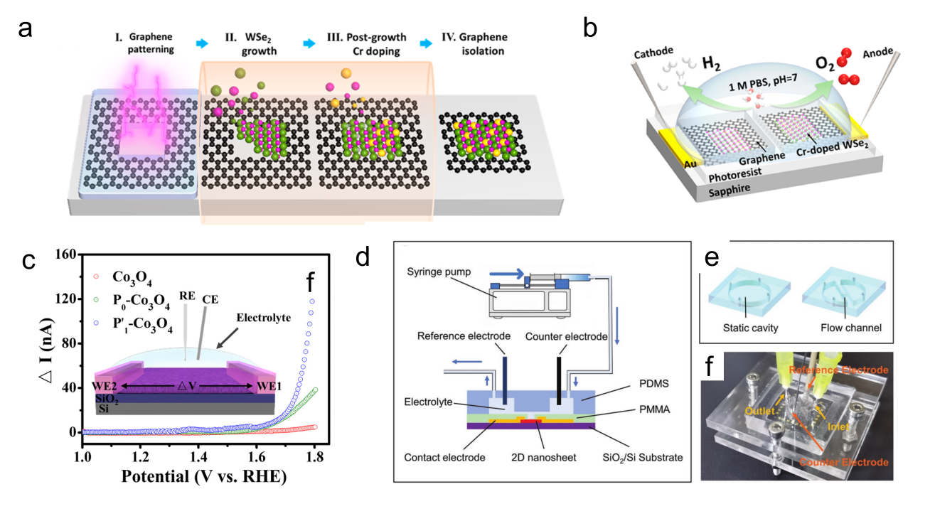
Figure 10.
(a) Schematic of the formation process of the Cr-WSe
2
/graphene heterojunction. (b) Schematic of the on-chip electrocatalytic device.
[
85
]
Copyright
2022
, American Chemical Society. (c) In situ I-V measurements of individual Co
3
O
4
, P
0
-Co
3
O
4
and P-Co
3
O
4
thin-films. Inset: The schematic of in situ I-V measurements. The applied potentials in WE1 and WE2 (called V1 and V2) increase synchronously vs. RHE, from 1 to 1.8 V, and keep the constant tiny potential difference ΔV (ΔV=1 mV).
[
159
]
Copyright
2021
, Elsevier Ltd. All rights reserved. (d) On-chip electrochemical measurement setup for the ORR. (e) Schematic illustration of the setup. (f) Schematic diagram of the static and microfluidic PDMS cells.
[
84
]
Copyright
2022
, Wiley-VCH Verlag GmbH & Co.
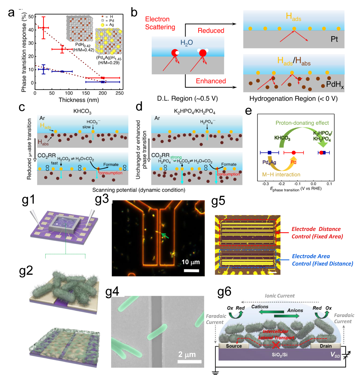
Figure 11.
(a) The relationship between the thicknesses of Pd and Pd
4
Ag nanowire films and their phase transition responses (ΔR
MHx
) is illustrated on the ETS. (b) Schematic of electron scattering in metals with surface adsorbates and hydrides. A schematic of the different Pd-H states in (c) KHCO
3
and (d) K
2
HPO
4
/KH
2
PO
4
and the corresponding CO
2
RR processes at the interfaces. (e) Summary of phase transition potentials of Pd and Pd
4
Ag under CO
2
RR conditions in KHCO
3
and K
2
HPO
4
/KH
2
PO
4
obtained at 10 mV/s.
[
172
]
(g1, g2) Schematic of the nanoelectronic measurement setup. (g3) Optical microscope (OM) image of MR-1 in dark-field mode. (g4) An ex situ SEM image of MR-1. (g5) Schematic of biofilm measurements. (g6) Schematic of the electrochemistry model at the interface of Shewanella oneidensis MR-1.
[
173
]
Copyright
2016
, American Chemical Society.
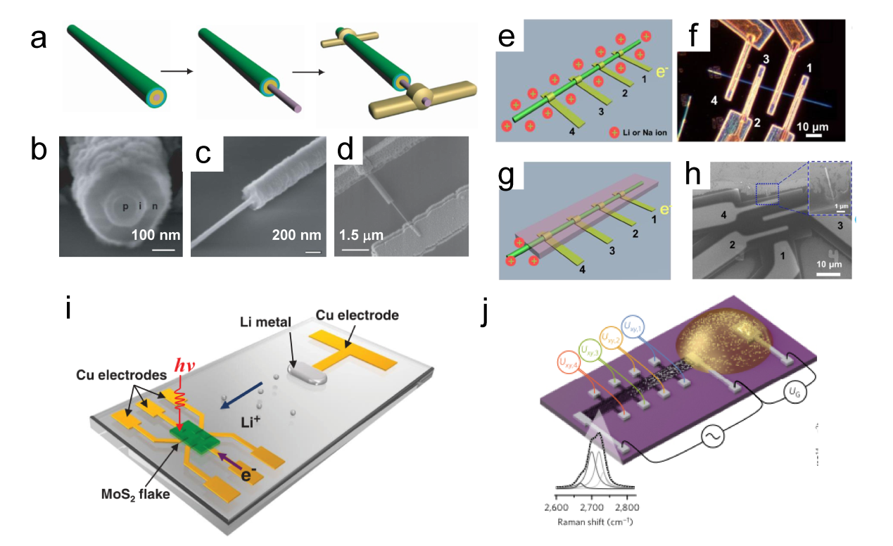
Figure 12.
(a) Schematics of fabrication process of the single nanowire photovoltaic device. (b, c, d) SEM images corresponding to schematics in a.
[
91
]
Copyright
2007
, Nature Publishing Group. (e, f) The schematics and dark field optical microscopic image of the nanowire electrode. (g) The second configuration, in which the nanowire is covered by a passivation layer with only one exposed end. (h) The SEM image of the device with the second configuration.
[
79
]
Copyright
2015
, American Chemical Society. (i) Schematic of MoS
2
-Li microbattery.
[
180
]
Copyright
2015
, Wiley-VCH Verlag GmbH & Co. (j) Schematic of the device for lithium ion diffusion in bilayer graphene. The inset shows the Raman scattering response of bilayer graphene.
[
181
]
Copyright
2017
, Nature Publishing Group.
Figure 13.
(a) Illustration of atomic defects observed in single-layer V-MoS
2
. (b) Statistical analysis of the concentration of these atomic defects.
[
116
]
Copyright
2022
, Wiley-VCH Verlag GmbH & Co. (c) Structural diagram of P-Co
3
O
4
. (d) Total electronic density of states for Co
3
O
4
and P-Co
3
O
4
. (e) Calculated PDOS of Co
3
O
4
and P-Co
3
O
4
. (f) Calculated free energy diagram of the OER on Co
3
O
4
and P- Co
3
O
4
.
[
159
]
Copyright
2021
, Elsevier Ltd. All rights reserved. (g) The schematic of the S vacancy site created on the modeled MoS
2
surface. (h) The computed band structures of the MoS
2
surface with 5.5% S vacancies at various induced charge levels. (i) The charge density difference of a monolayer of MoS
2
with 5.5% S vacancies.
[
192
]
Copyright
2019
, American Chemical Society.
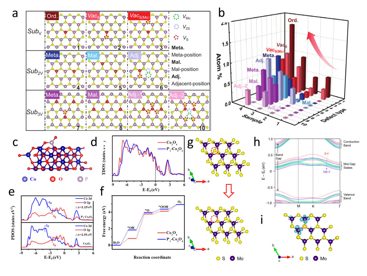
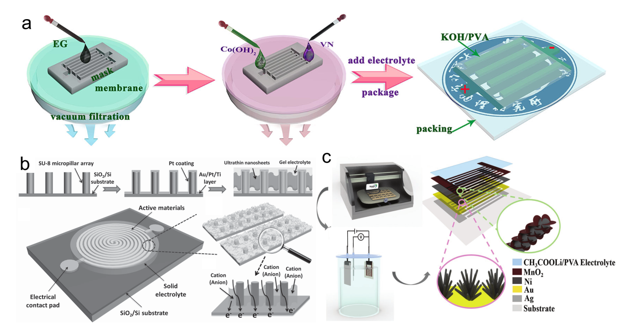
Figure 14.
(a) Fabrication and structural characterization of SST-MPCs.
[
205
]
Copyright
2018
, Nature Publishing Group. (b) Schematic of the fabrication process of SST-MPCs.
[
206
]
Copyright
2015
, Wiley-VCH Verlag GmbH & Co. (c) Schematic of the printable fabrication procedure.
[
207
]
Copyright
2017
, Wiley-VCH Verlag GmbH & Co.
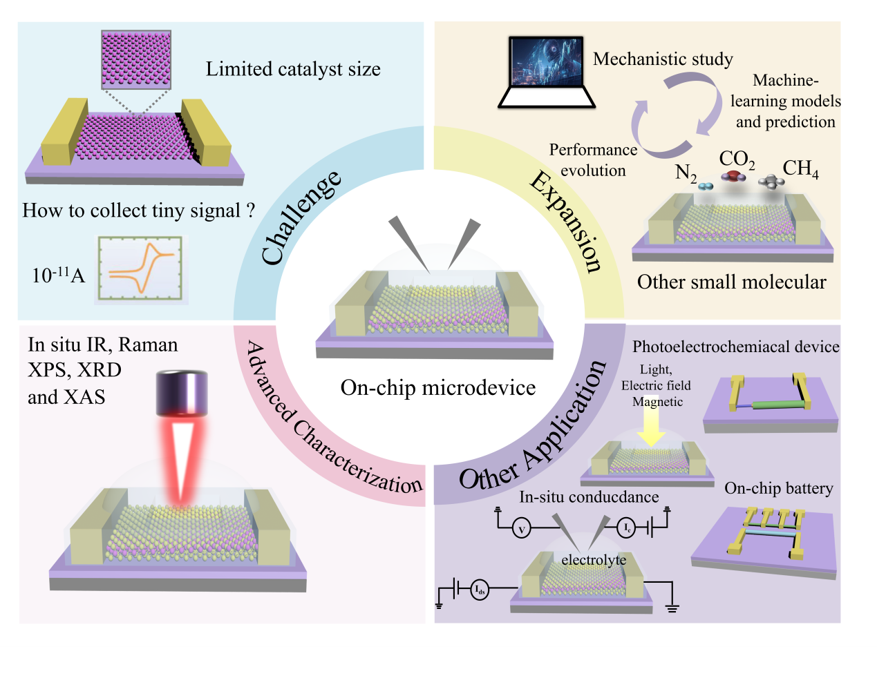
Figure 15.
Prospects for on-chip microcells. The challenges in this emergent field, such as limited catalyst size. The applications of the on-chip microcells, e.g., the expansion, other application and advanced characterization are expected.