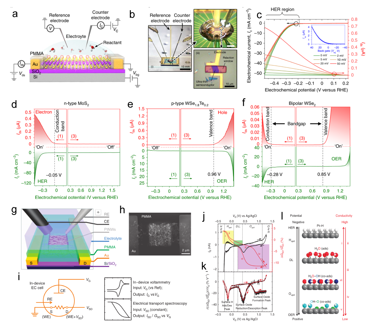
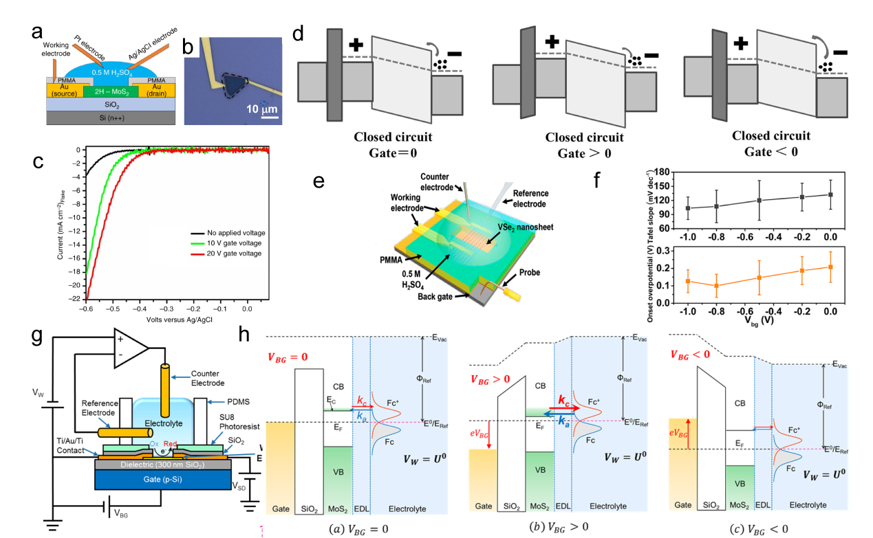
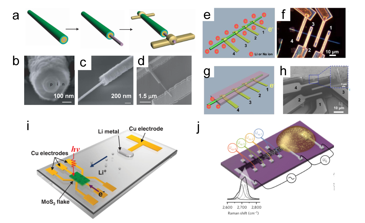
Figure 8. (a) Schematic of the microcell-based in situ electronic/electrochemical measurement. (b) Optical image of the microcell. (c) Typical electrochemical (y axis in black) and electronic (y axis in red) signals of single-layer WS2 during the HER at different bias potentials. Self-gating phenomenon of (d) n-type MoS2, (e) p-type WSe1.8Te0.2, and (f) bipolar WSe2, typically, n-type MoS2 is turned on at a negative electrochemical potential and only delivers the HER, p-type WSe1.8Te0.2 is turned on at a positive electrochemical potential and only delivers the OER, bipolar WSe2 is turned on at both negative and positive electrochemical.[69] Copyright 2019, Nature Publishing Group. (g) Schematic of the Pt NW device. (h) SEM image of the device cell. (i) Schematic of CV and ETS for in situ monitoring of the electrochemical interfaces. (j) The IG-VG and normalized GSD-VG characteristics of a typical Pt NW device, IG-VG resembles the typical CV characteristic of a polycrystalline Pt surface, containing redox regions of HER, H adsorption/desorption region (Hupd), double layer (DL) region, surface oxide formation/reduction region (Oupd) and OER. (k) The differentiated ETS curve illustrates spectral peak characteristics. (l) Schematic of various Pt surface conditions along with the sweeping electrochemical potentials (left black axis) and the corresponding changes in conductivity.[68]
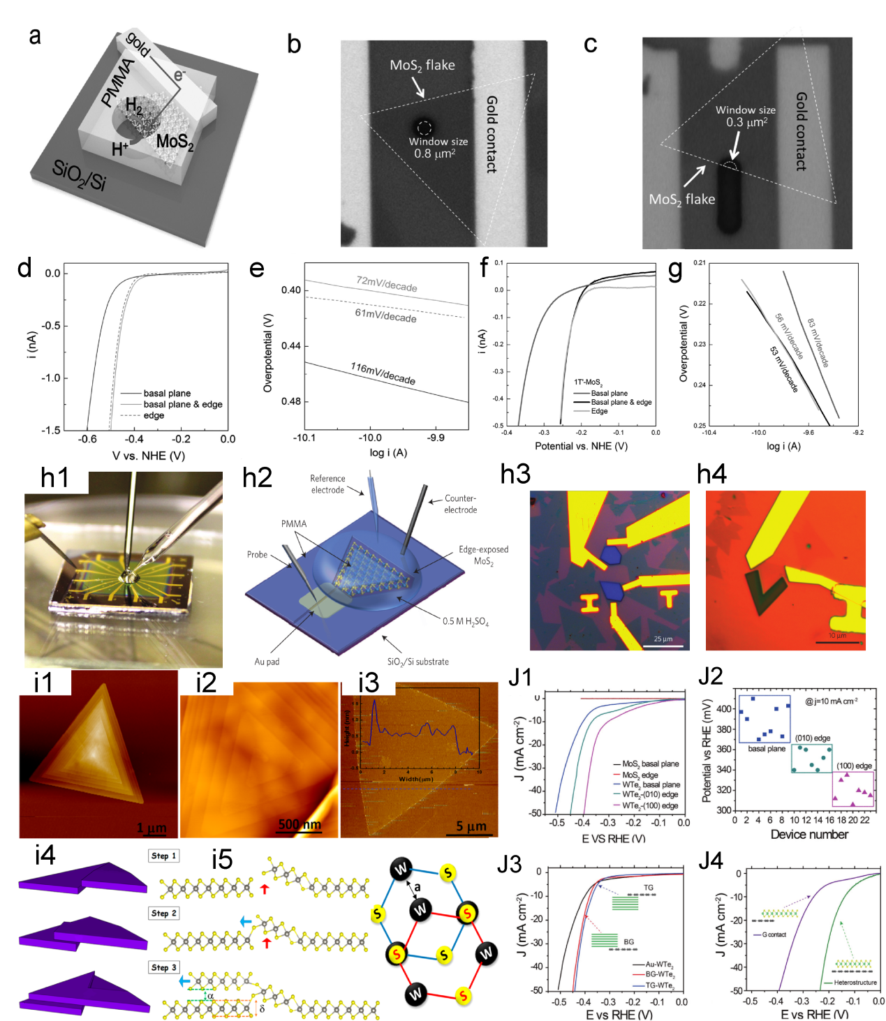
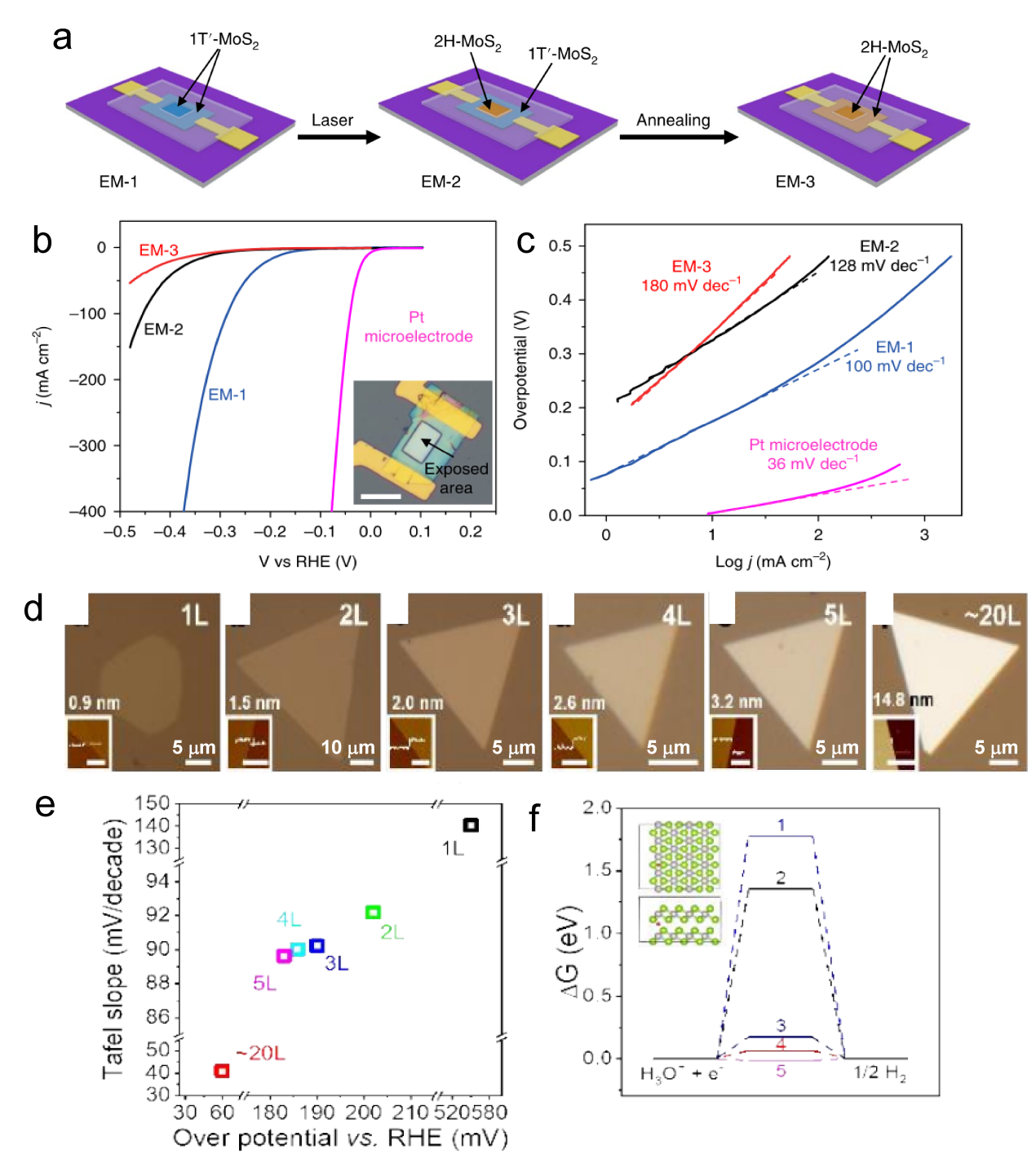
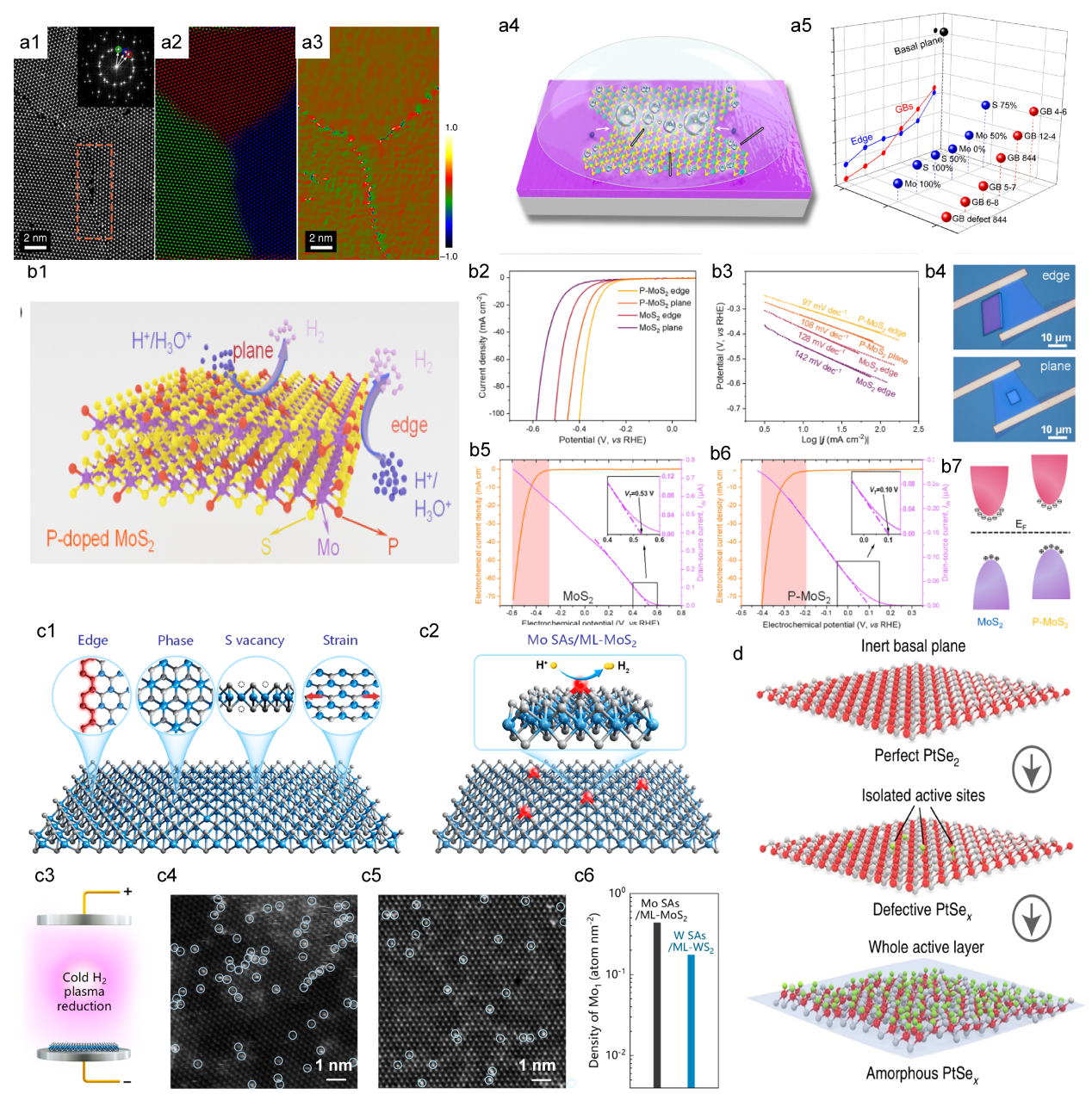
Other figure/table from this article