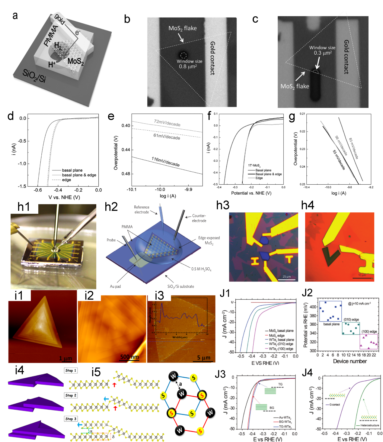
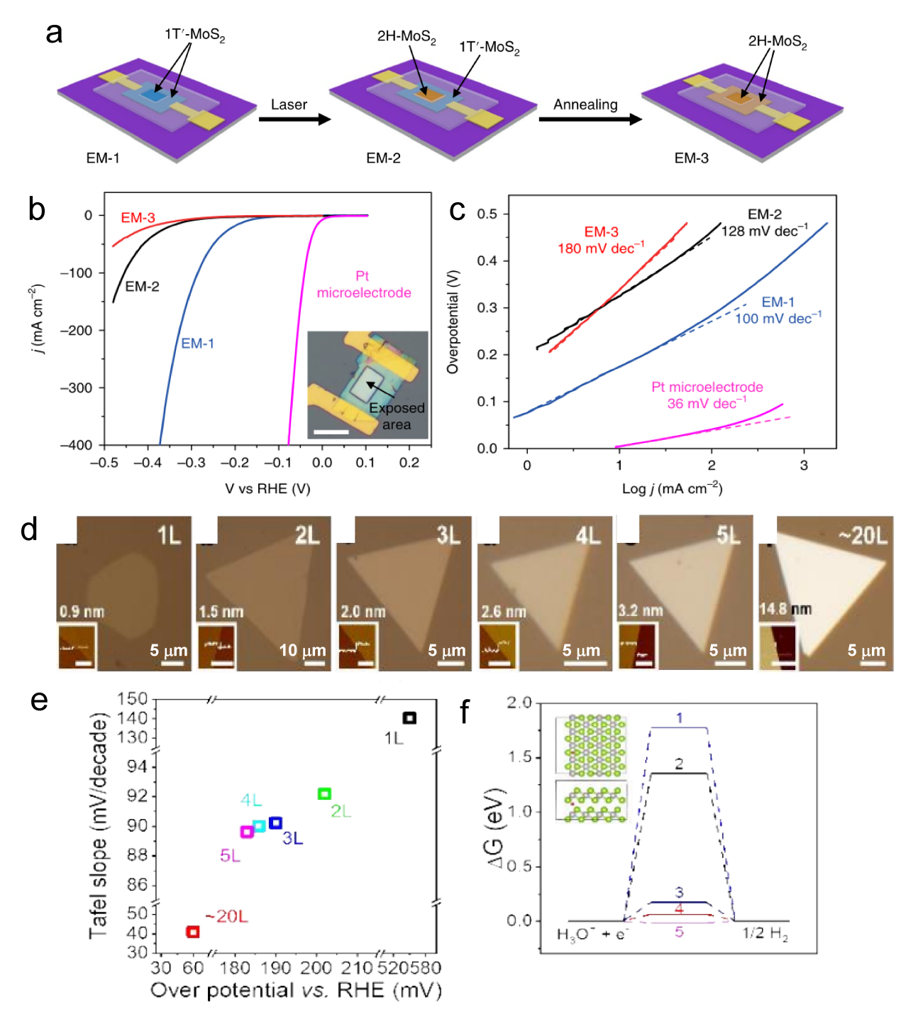
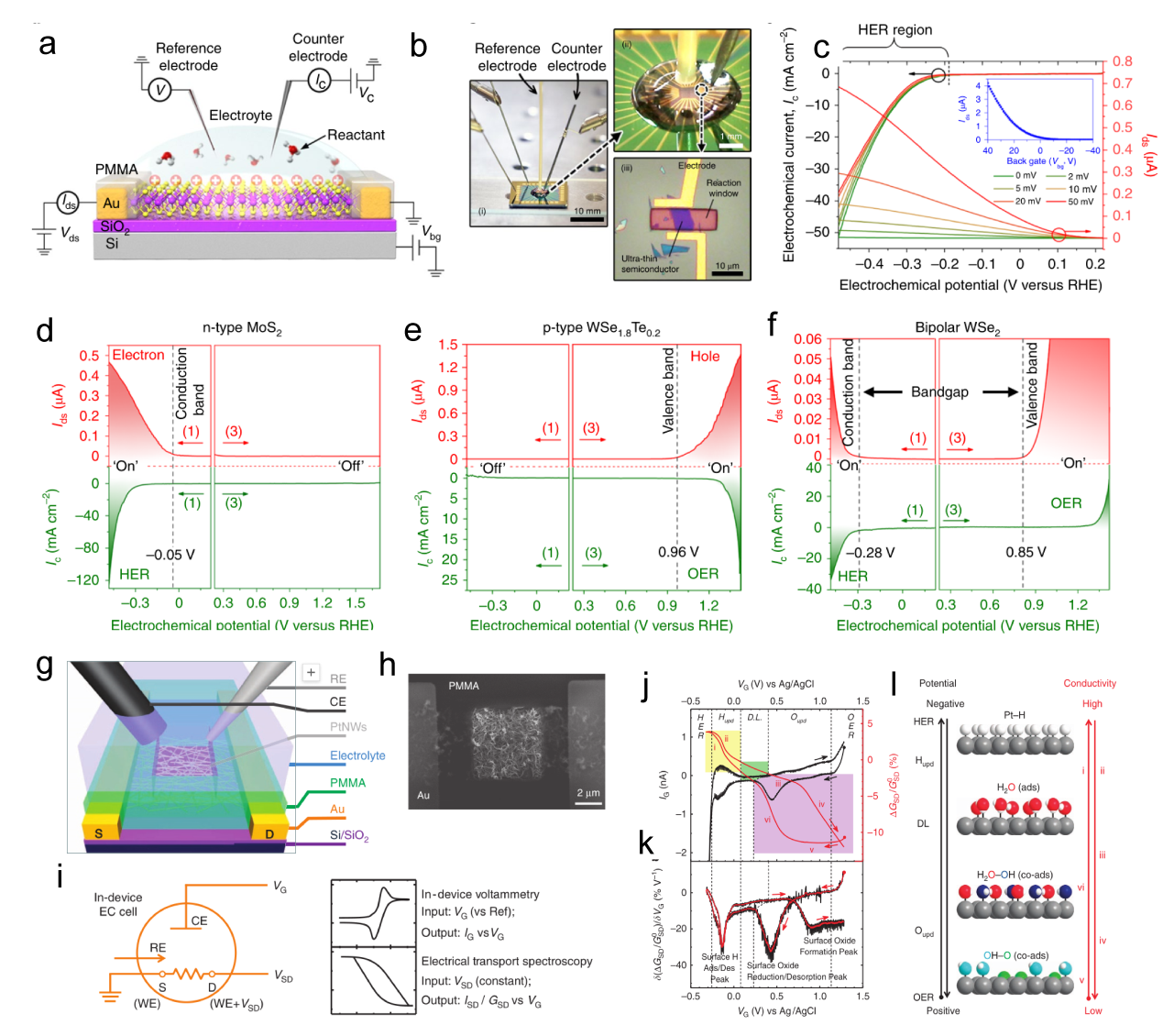
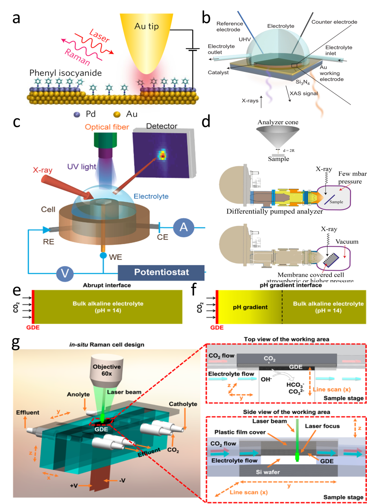
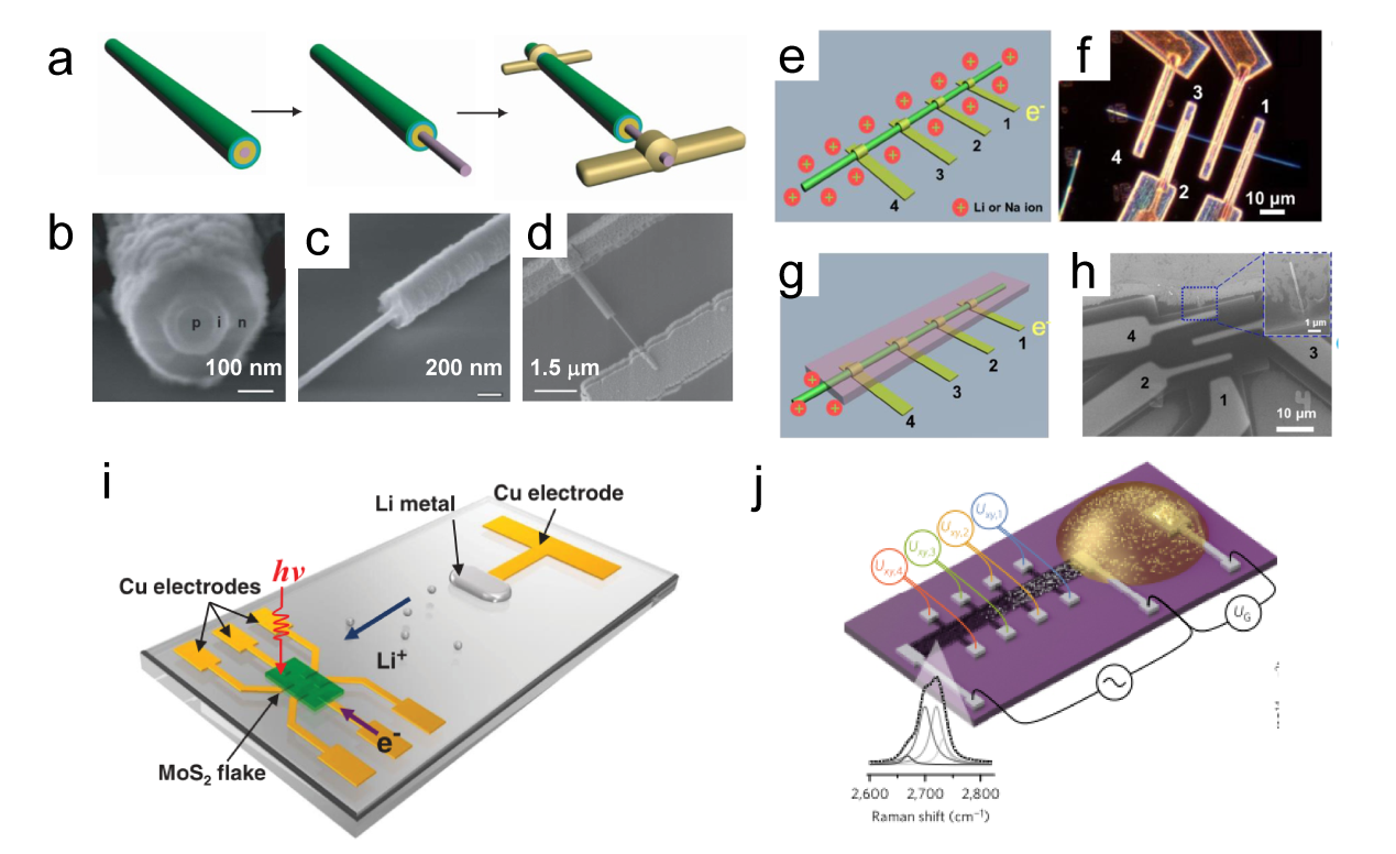
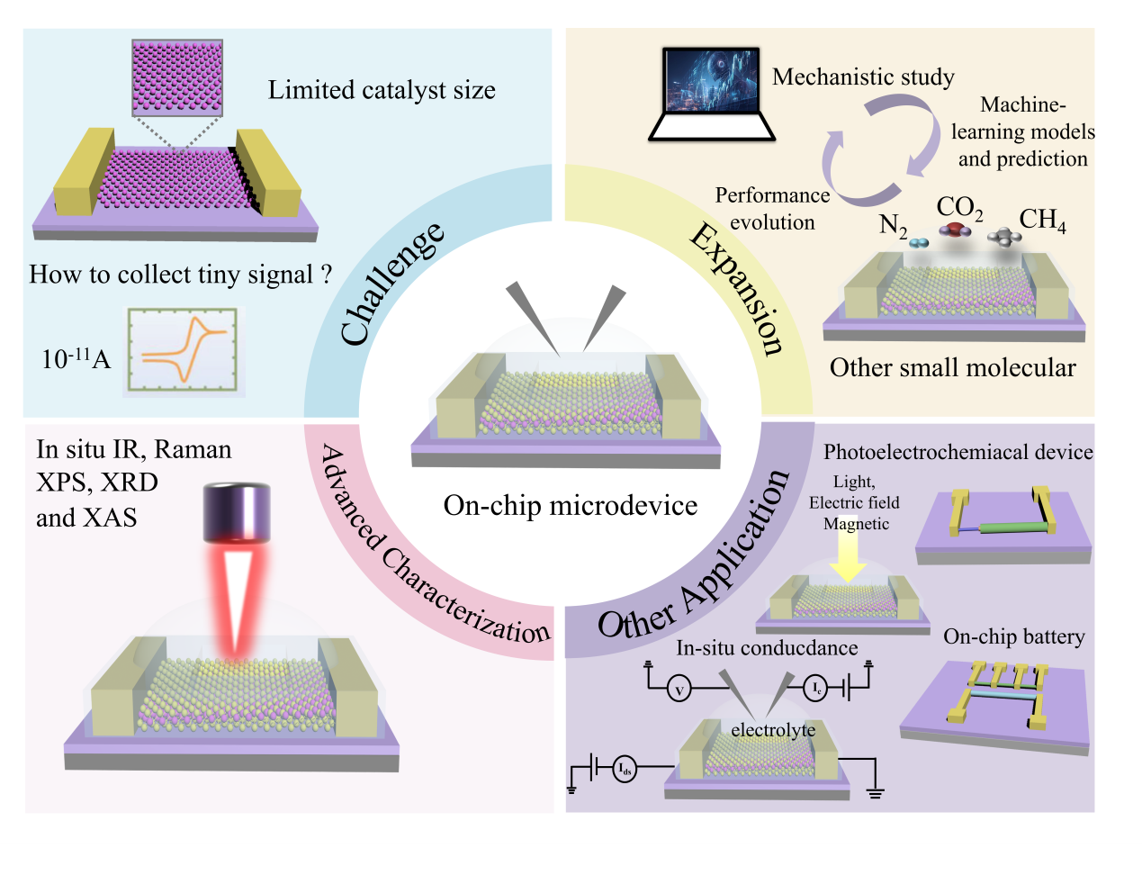
Figure 4. (a) Schematic of the on-chip setup. Optical image of a MoS2 showing the (b) basal and (c) edge planes. (d) LSV and (e) Tafel plots of the MoS2 with basal plane and edge, the electrolyte was argon-purged in 0.5 M H2SO4 and scan rate was set at 10 mV s−1. (f) LSV and (g) Tafel curves of monolayer 1T′-MoS2 basal plane, and edge in HER.[64] Copyright 2017, Wiley-VCH Verlag GmbH & Co. (h1) Photograph of the electrochemical microcell. (h2) Schematic of the on-chip electrocatalytic. Optical microscope images of single-layer MoS2 with (h3) the basal and (h4) edge exposed.[80] Copyright 2016, Nature Publishing Group. (i1, i2) AFM of spiral WS2 domains and (i3) corresponding height of monolayer WS2. (i4) Schematic of the spiral domain growth modes. (i5) Schematic of the atomic arrangement in spiral WS2.[104] Copyright 2019, American Chemical Society. (j1) LSV of MoS2 and WTe2 with different exposed area, the overpotential of (100), (010) edge and basal plane is 320 ± 10 mV, 350 ± 10 mV and 390 ± 20 mV respectively at 10 mA cm−2. (j2) Summary of the overpotentials for WTe2 with different exposed sites. (j3) LSV of WTe2 with basal plane. (j4) LSV of MoS2 with a graphene contact, as well as from the MoS2/graphene heterostructure.[105] Copyright 2018, Wiley-VCH Verlag GmbH & Co.
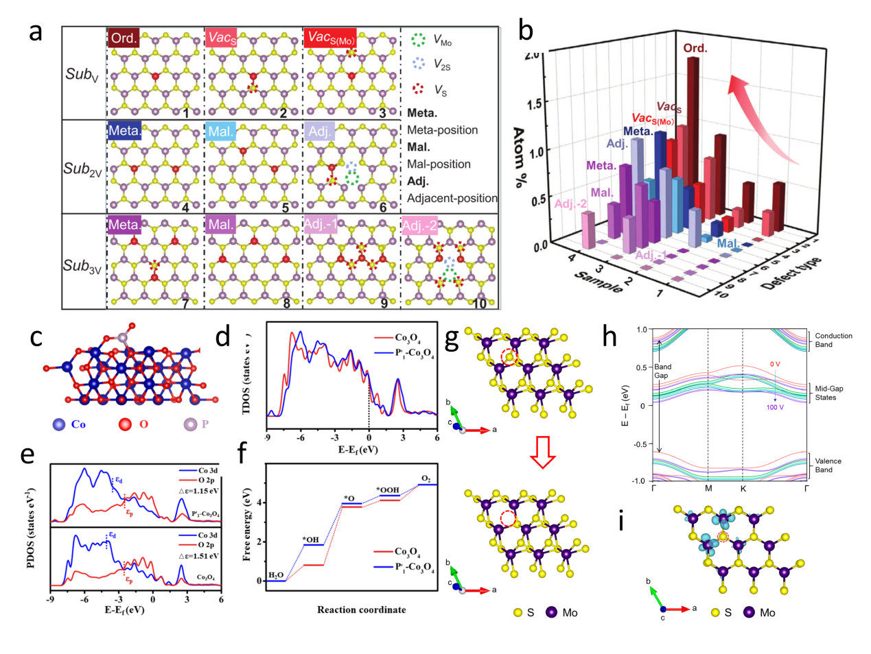
Other figure/table from this article