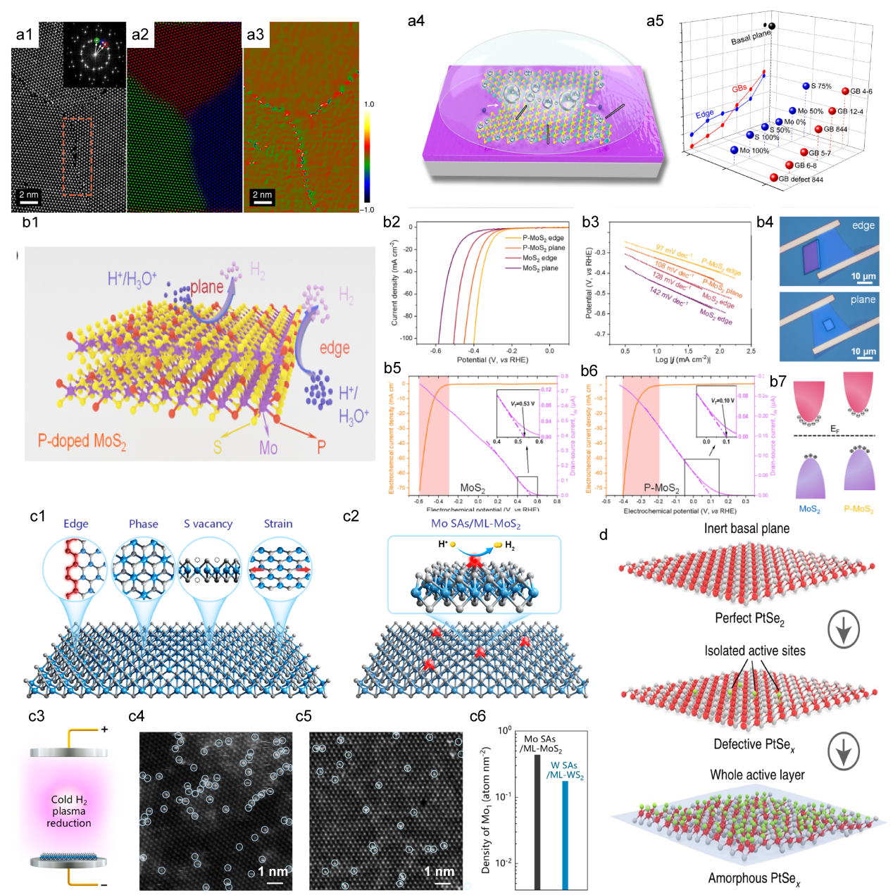
Figure 6. (a1) The HAADF STEM image of the GBs between three MoS2 grains, the inset on the left shows the Fourier transform. (a2) The composite color-coded inverse fast Fourier transform (IFFT) image. (a3) illustrates the Geometrical Phase Analysis (GPA) routine.[112] (b1) Schematic of HER process on P-MoS2 nanosheets. (b2) and (b3) show the LSV and Tafel plots for the MoS2 and P-MoS2, The edge sites show an onset potential (η10) of 297 mV and a Tafel slope of 97 mV dec−1 for HER, exceeding those of the basal plane with 328 mV and 108 mV dec−1. (b4) Optical images of edge and basal plane on a P-MoS2. (b5) and (b6) display the electrochemical and electronic signals of a MoS2 and P-MoS2 during the HER. (b7) Illustrates the electronic structure of P-MoS2, aligning the Fermi levels.[113] Copyright 2017, American Chemical Society. (c1) Schematic of the active sites of MoS2. (c2) Schematic of Mo ML-MoS2. (c3) Details the synthesis of metal SAs on a ML-MoS2. HAADF-STEM images in panels (c4) and (c5) depict Mo SAs on ML-MoS2 and tungsten SAs on monolayer WS2 samples, respectively. (c6) statistical results on the density of Mo and W SAs on 2D monolayers.[114] Copyright 2020, American Chemical Society. (d) Schematic of the amorphous PtSex surface, perfect PtSe2 and defective PtSex.[115] Copyright 2022, Nature Publishing Group.
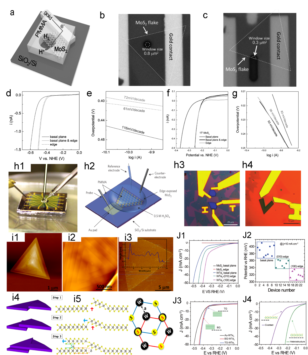
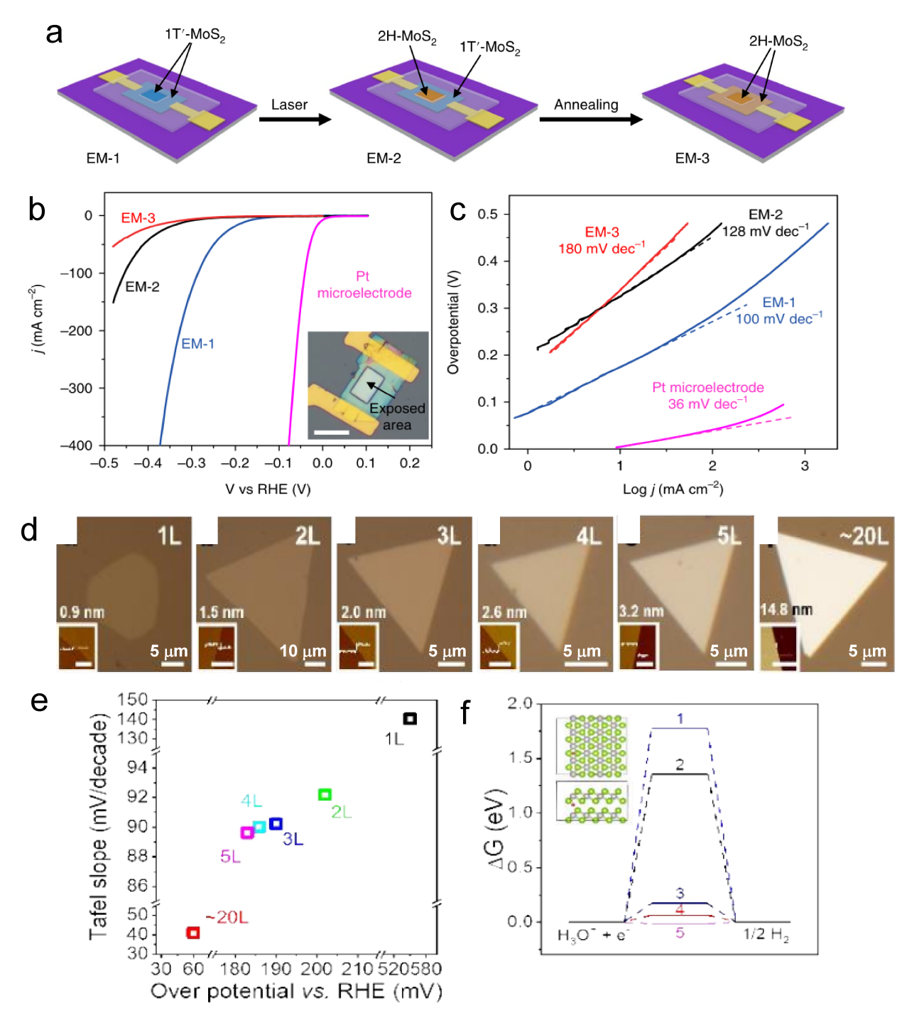
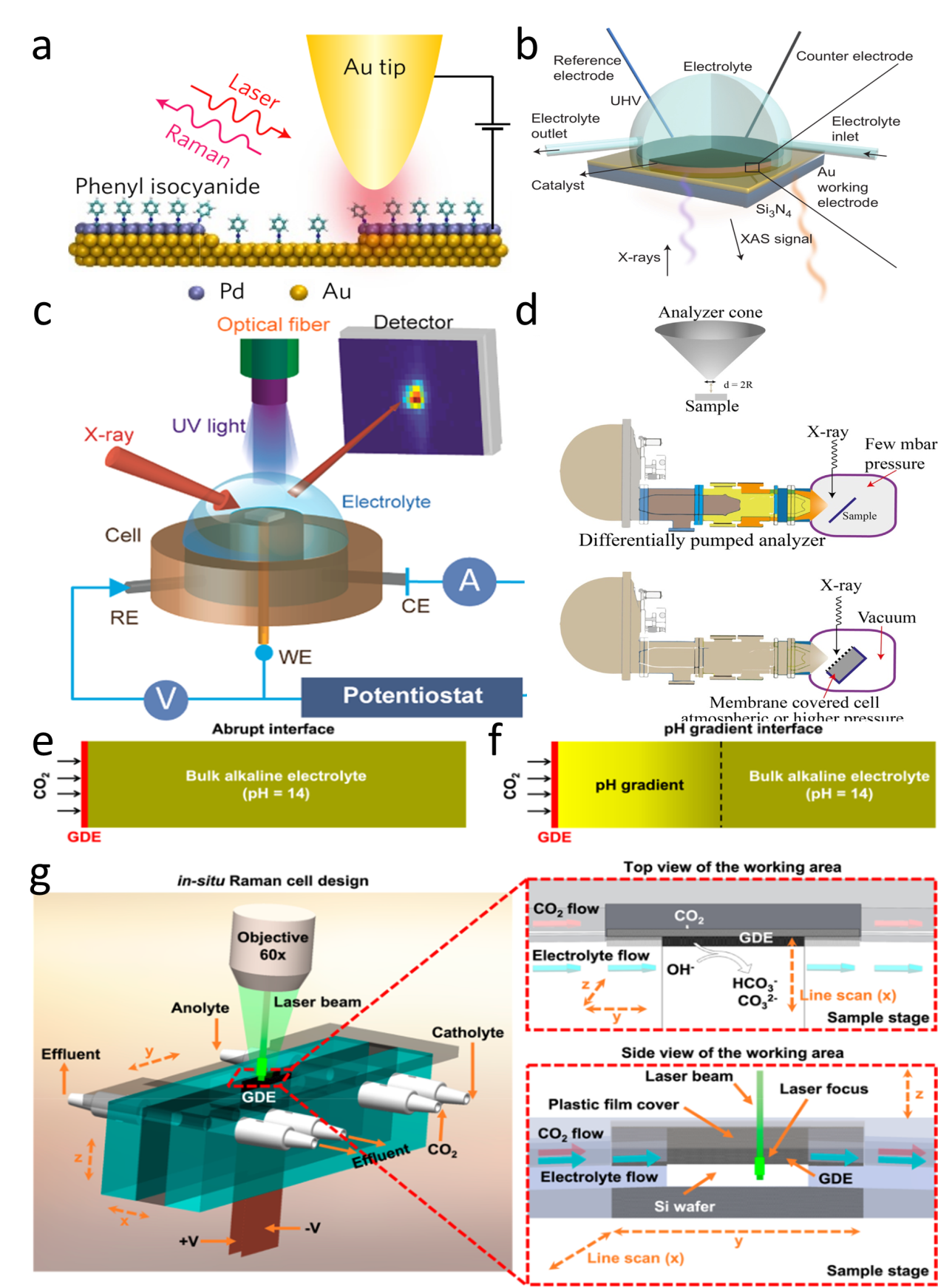
Other figure/table from this article