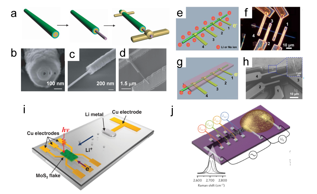
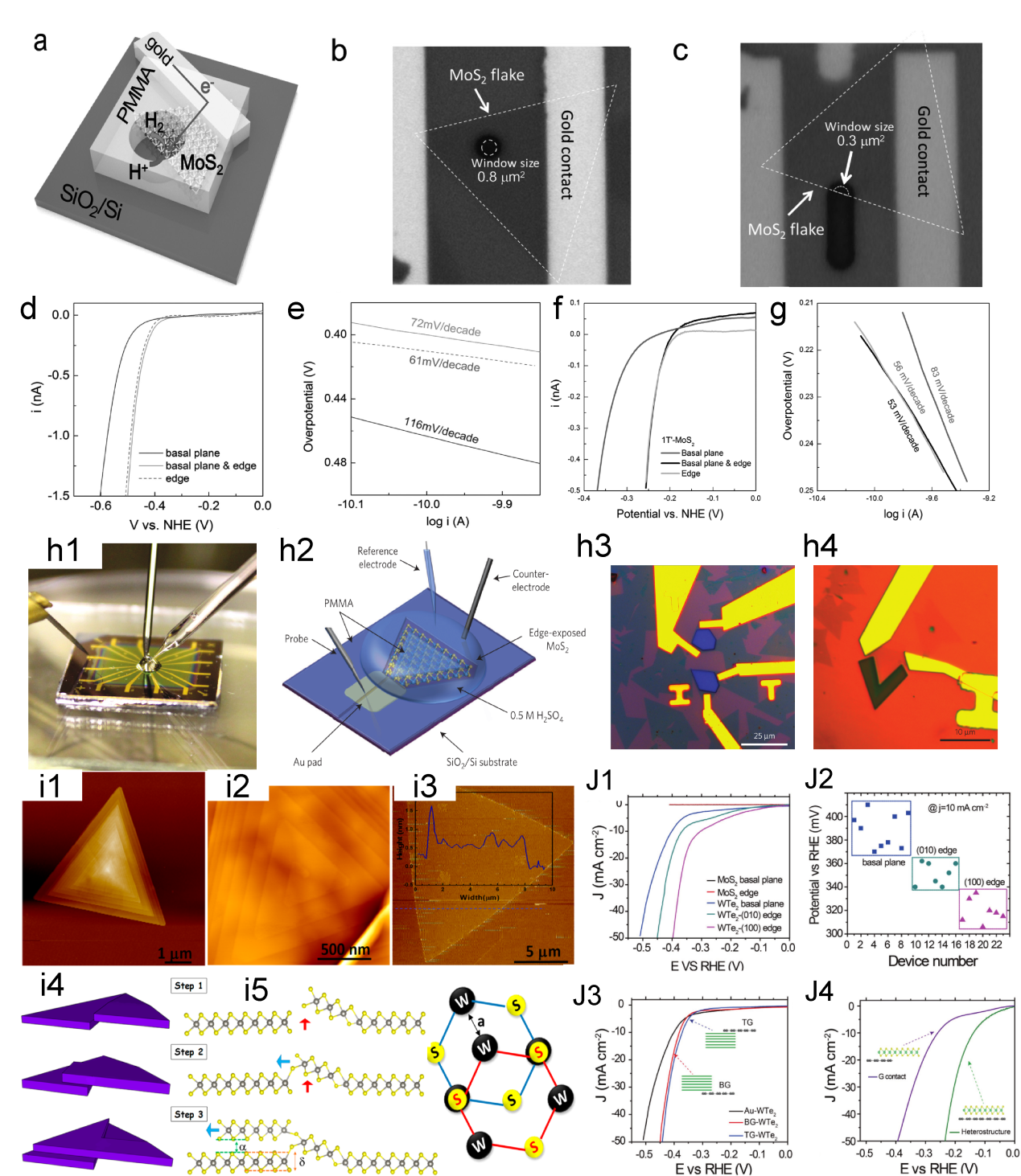
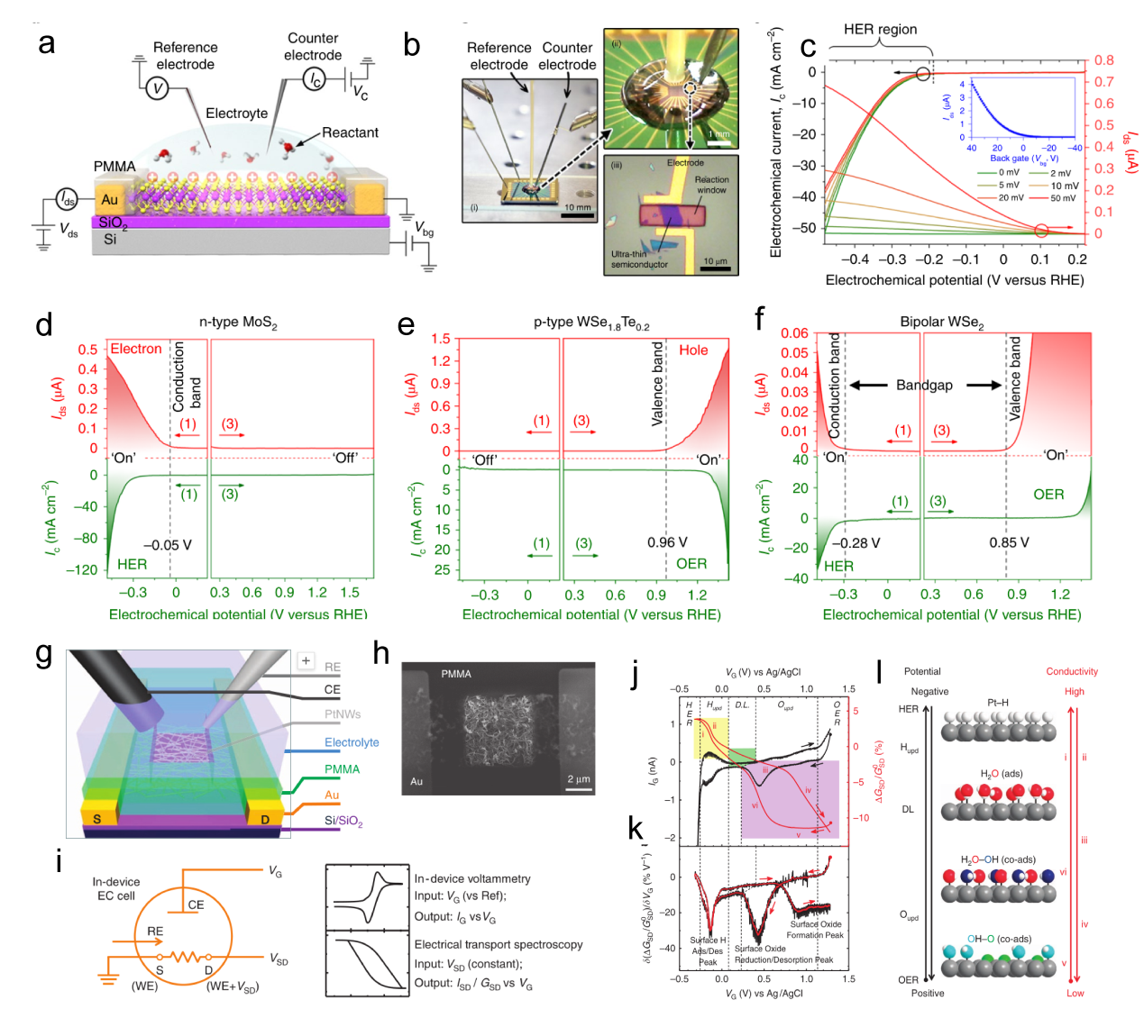
Figure 12. (a) Schematics of fabrication process of the single nanowire photovoltaic device. (b, c, d) SEM images corresponding to schematics in a.[91] Copyright 2007, Nature Publishing Group. (e, f) The schematics and dark field optical microscopic image of the nanowire electrode. (g) The second configuration, in which the nanowire is covered by a passivation layer with only one exposed end. (h) The SEM image of the device with the second configuration.[79] Copyright 2015, American Chemical Society. (i) Schematic of MoS2-Li microbattery.[180] Copyright 2015, Wiley-VCH Verlag GmbH & Co. (j) Schematic of the device for lithium ion diffusion in bilayer graphene. The inset shows the Raman scattering response of bilayer graphene.[181] Copyright 2017, Nature Publishing Group.
Other figure/table from this article